CSE 140L Lab 1 - Combinational Circuit Design
Spring 2009, Professor Cheng, TAs Thomas Weng, Renshen Wang, Chengmo Yang, Mingjing Chen
Due time: Demonstrate by Friday 4/24, Report due Friday 4/24 11:59PM Check webboard for details on postponement! (through WebCT, http://webct.ucsd.edu)
Important! Please regularily check http://webboard.ucsd.edu for the latest updates and news regarding this lab. FAQs and announcements will be on the webboard, so check it often! Also, please get started sooner rather than later. This lab should take a bit more than 4 hours to do (assuming you understand the material), but since you must demonstrate this for us, you should be done before Wednesday.
CSEL tutorial updated with corrections
Objective
- Learn and become familiar with the Altera Quartus II FPGA EDA tool.
- Learn how to design basic combinational digital components such as adders and multiplexers.
- Learn how to download designs onto the FPGA platform.
- Learn how to do functional and timing simulations and to examine the resulting waveforms.
Note, the first parts of this lab are almost entirely given to you in step by step
instructions. The objective is for you to learn how to use Quartus II
and the basic steps in designing a combinational circuit from
specification to testing. That being the case, please make sure that
you understand everything that you do in this lab!
Important: Note, on the screen shots you will see that we have an CycloneII EP2C35F as our target
FPGA. That is because we (the TAs) have the DE2 board. You guys will likely be using a DE1 board,
which has a different CycloneII FPGA, the CycloneII EP2C20F484C7. When you guys pick your target
FPGA, make sure you pick the correct one! When in doubt, look at your board and manual to see the acutal number.
The DE1 manual is on your CD-ROM, and it's also on the web at: Altera DE1 Manual.
Another good resource is this
Altera DE2 tutorial .
Please make sure you have Quartus II 9.0 from the Altera
website. The version on the cdrom is 8.1, please do not use that.
Part 1. Introductory Tutorial
Follow along with the following tutorials, making sure that you
understand each step. You will learn the basics of your hardware
platform and the Quartus II EDA program. Tou will also learn how to
design a very basic combinational circuit and simulate it on the actual
FPGA board. If you do not understand a step, please ask a TA for help.
Relevant chapters in the book are Chapters 2 and 3.
Software and Hardware Introduction
Basic Combinational Circuit Tutorial
Report:
- Write a short summary (max 100 words) of the
overall process of using Quartus II to design a simple combinational
circuit, and getting it to work correctly with your FPGA board.
Part 2. Spell C S E L on the Segment Display
In this part, you will design and run a circuit that will
display C S E L (short for CSE 140L) on the board's segment display, depending on what
button combination you have pressed. Follow along with the following
tutorial to build and run your circuit. Note the processes that you do
in order to design a circuit. Even though this part is mostly given to you,
please make sure you understand each step.
C S E L Segment Display Tutorial
Report:
- Include schematic diagrams of your circuit
- Include your full truth table for CSEL. One row is given to you in the tutorial, provide the full truth table.
- Include the boolean expressions you derived from the truth table. Two were already given to you.
Part 3. Output 1-Bit Numbers with the Segment Display and Switch Input
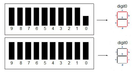
In this part, you will learn to use the 10 switch input. You
will design a combinational circuit that will display the number
corresponding to the 1-bit value associated with switch 0. Thus, if
switch 0 is pressed down, then your digit 0 should show
0, and if switch 0 is in the up position, your digit 0
will show 1.
After you have made your circuit, you will create a module
for it in part 4, as you will use the 1-bit number displayer for your
adder. Note, this means you will ignore switch inputs 1 through 9, and only
focus on input 1 on your switch. Again you can ignore digits 1, 2, and 3. This circuit is extremely easy to do
and should take you no more than 30 minutes maximum.
Report:
- Include schematic diagrams of your circuit
- Include the truth table that you used to derive the appropriate outputs.
- In this part, you only worried about 1 input, so you only
displayed 0 or 1 on the segment display. What if we had 3 inputs (and
thus 3-bits)? With only 1 bit, we only have two values - 0 and 1. But with
3-bits, we have 8 possible values, 0-7.
So Instead of using just switch input 0, we used input 0, 1, and 2. Then
you would display 0 to 7 on the segment display, instead of just 0 or
1. Write out the truth table for this. (Hint, it is similar to what you
did in part 2 to figure out the segment display for CSEL, except now
you have 3 inputs instead of 2). You don't have to do this on Quartus, you
just have to write this out.
Part 4. 4-bit Ripple Carry Adders
In this part, you will design a 4-bit ripple carry adder. You will learn how to
create a module with a combinational circuit, and how to use that
module in higher level circuits. By breaking up a combinational circuit
into modules, you can begin to design more complicated circuits. You
will use your 4-bit number displayer from part 3 to display the results
on the segment display.
A 4-bit adder will add two 4 bit numbers to get a 4 bit result as well as a 1-bit carry out.
Because your DE1 board only has 4 digits, we will have to ignore that 1-bit carry out.
You will run your adder circuit on the FPGA board. The three inputs
of the full adder, A0-A3 and B0-B3, will be the switches 0-3 for A,
and 6-9 for B, on the board; the output S0-S4 will be displayed on the 4 digit displays.
An included tutorial will help guide you, but by now you should know
how to design a circuit and thus less detail will be given.
Adder Tutorial
Report:
- Include schematic diagrams of your circuit
- Include functional and timing diagrams of your simulation for your full adder. You do not have to provide simulations for your 4-bit adder.
- What is the worst case delay through the 4-bit adder? (That is, what path from an input to its destination output causes the longest delay in your circuit?) Figure out what inputs make this happen. You can write this out and explain it.
Part 5. Multiplexers
A 2-to-1 multiplexer (MUX) selects one of the two input signals according to the control signal:
Input: data signal A and B; control signal ctrl.
Output: signal C;
Function: C=A if ctrl=0; C=B if ctrl=1.
In this assignment, you are required to do the following tasks:
1. Build a 2-to-1 multiplexer using logic gates.
2. A 4-to-1 MUX selects one of the four input signals according to the control signal. Define the specification for this 4-to-1 MUX, i.e., input, output & their relationship.
3. Build the 4-to-1 MUX using the 2-to-1 MUX built in step 1. Demonstrate your work on the board. Use two push buttons as the control lines and switches 0-3 as inputs. Display the outputs on digit0. For example, if switch 0, 1 are 0 and 2, 3 are 1, then the display will show 0 if the push buttons are (0,0) or (0,1) and will show 1 for the other 2 combinations of button inputs.
Report:- Specification of the 4-to-1 MUX;
- Schematic diagrams of the 2-to-1 MUX and 4-to-1 MUX;
- Functional and timing diagrams of your simulations for the 4 to 1 MUX.
Demonstration
For your demonstration, you will
need to demonstrate part 4 and 5 to one of the TAs.
Please look at the office hours for when we are available. Note, you can
contact us if those times do not work, as we are happy to meet you outside
those times too durning the evening. There are several ways you can
demonstrate your board to us. First, bring your board and a laptop with your
project files and Quartus to any of the TAs during their office hours.
Demonstrate part 4 to us, and then reprogram your board with part 5. The TA
will check both parts are working and mark your name down. Check out the demonstration
page to see more details on how to demonstrate to us your circuit.
Alternatively, if you come see me (Thomas) during my lab hours, you can use my
laptop to reprogram the board, or one of the lab computers. In this case, bring
your project files on a USB drive or email it to yourself so you can retrieve it
on the computer.
If all looks good, we
will give you thumbs up. If something doesn't work correctly, then
please go back and fix it.
Report Instructions
You lab report should include:
- Title page, which contains Names and PID of students, due date,
title of lab, and brief discription of each person's contribution.
- Part 1 - answers
- Part 2 - schematic diagrams, answers
- Part 3 - schematic diagrams, answers
- Part 4 - schematic diagrams, functional diagrams, timing diagrams, and answers
- Part 5 - schematic diagrams, functional diagrams, timing diagrams, and answers
Grading
20% of your grade will be from the demonstration, so this is an
easy 20%. Another 40% will be in your logic schematics and timing
diagrams. Easy points assuming you were able to demonstrate this for
us. 30% will be in your answers to the questions.
Final Notes
Good luck with your lab! Also please run through the interactive
tutorial if you haven't before. Now that you have a good familiarity
with the software and system, you can go through some of the guides
with a better grasp than before. There are some other good software
tutorials online as well, on the Altera Quartus II webpage. Being able
to use EDA tools like Quartus II is important for this class, and will
be even more important for CSE141L. By now you should be able to:
1) Run Quartus II and open and create new projects.
2) Draw some logic design using the buttons and switches as inputs, and the segment display as outputs.
3) Create a module, and use that module in other schematic designs.
4) Download and test your design on your FPGA board.
5) Run simulations with your circuit and understand the functional and timing diagrams.