-
Build a connection between design flow in theory and a pratical design tool

-
Design basic combinational logics
-
Start Xilinx ISE 6 (Project Navigator)
-
Create a project
-
Working directory
-
Project name
-
Module type
-
Device
-
Add half_adder
-
Put an AND gate and a XOR gate
-
Connect them
-
Add input/output ports
-
Create a symbol
-
Add full_adder
-
Put two half_adder instances and one OR gate
-
Connect them
-
Add input/output ports
-
Add simulation inputs file
-
Synthesize
-
Implement
-
Simulate
-
Start Modelsim
- Check Timing
How to download and install ISE WebPACK 7.1 with ModelSim XE III Starter?
-
Create your Xilinx account.
www.xilinx.com -> SUPPORT -> MySupport -> Login/Register (http://www.xilinx.com/support/mysupport.htm) -
Download ISE WebPACK 7.1 and ModelSim XE III Starter(6.0a).
www.xilinx.com -> Products&Service -> ISE Design Tools -> ISE WebPACK -> Download (http://www.xilinx.com/webpack/index.htm) -
Install ISE WebPACK 7.1 and ModelSim XE III Starter.
-
ISE WebPACK single file installation is preferred.
(ISE WebPACK 7.1 WebInstall is quite slow.) -
Install ModelSim XE III Starter. (NOT full version)
-
Licensing ModelSim XE III Starter.
-
Request license.

-
Fill in your information, a license file "license.dat" will be sent to you by email.
-
Start License Wizard.

-
Indicate your license file location.

-
Follow the instructions to finish license setup.

- Installation finished. Start Xilinx Project Navigator.
To identify one bit position among four, we need two address bits.

Asssume there is a 2-bit counter giving a sequence '00', '01', '10' and '11', the 4-bit parallel data will serially appear at the output of a 4-1 MUX.
Following is a diagram of 4-1 MUX.

Back to Top
Intuitively the destination changing should reflect the changing at the source input, and no other input will disturb the destination status. That means all other inputs won't change and let the source input signal go through the critical path.
Here's an example of 4-bit adder.

Assume the critial path is from Ci to S3. All A0A1A2A3 and B0B1B2B3 are fixed, so that the changing of S3 only reflect the act of Ci, not A2. Also Ci should be allowed to propogate to S3. We can set A0A1A2A3=1110 and B0B1B2B3=0000:
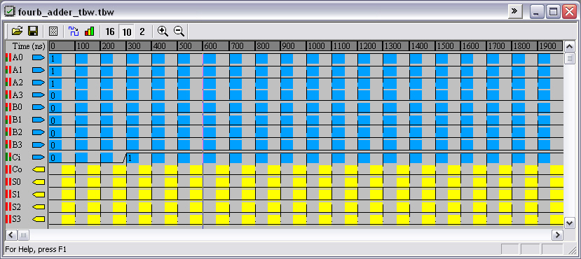
We expect a positive edge at S3 after 300ns. The following is the simulation result. The distance between the stimulation and the response is the critical path delay.

Back to Top
A critical path is a path from an input to an output with the largest delay. Xilinx timing analysis tool provides a good way to identify critical paths. It analyses every path from the input to the output, and gives the delay on each path. We can easily find the critical path from the timing report.
The following is an example to find a critical path in a full adder design:
- Choose your component
Highlight your four-bit adder source file (e.g. four_bit_adder.sch) in the project source window of the Xilinx Project Navigator.
- Generate the timing report
In the process view window, click on the ?Implement Design -> Generate Post-Place and Route Static Timing -> Post-Place and Route Static Timing Report ?step. A timing analyzer window shall pop-up with the timing report similar to the following:

-
Identify the critical path
The critical path is from input B to output S, with a delay of 6.428 nanoseconds, according to the timing report.
We shall be able to get the critical path delay from simulation waveforms. Using a test bench waveform with single toggle at input B, we get the simulation wave forms as follows. Note that the exact 6.428 ns delay is shown in the waveforms.
 |
A 4-bit adder takes as input three numbers, A , B and Ci , sum them up, and generates two output numbers, S and Co . Numbers A, B , and S are 4-bit binary numbers: A = (a3a2a1a0); B = (b3b2b1b0); S = (s3s2s1s0). Ci and Co are single bit binary numbers. A and B are two operands of the addition operation. Ci is the carry-in bit. S is the sum. Co is the carry-out bit.
Back to Top
- Download ModelSim XE III from http://www.xilinx.com/webpack/index.htm.
- In the installation, select ModelSim XE III Starter.

Select Full VHDL as library installation type.
Use default values for other options. - Integrate Modelsim with Xilinx ISE. (Usually it's done by Xilinx ISE automatically. But if you didn't see the ModelSim options when you click on a Test Bench Waveform file, please integrate ModelSim manually.)
- Click on the Edit menu in Xilinx ISE 7.1, and click on Preferences.
- In the Preferences window, indicate the ModelSim installation directory in Integrated Tools Options.

- Click OK.