Problem #1
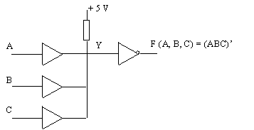
In this circuit when one (or more) of the inputs to the OC buffers is
(are) 0, Y = 0 and F = 1. In order to make F = 0 (Y = 1), all of the inputs
should be 1.
| A B C | F(A, B, C) |
| 0 0 0 | 1 |
| 0 0 1 | 1 |
| 0 1 0 | 1 |
| 0 1 1 | 1 |
| 1 0 0 | 1 |
| 1 0 1 | 1 |
| 1 1 0 | 1 |
| 1 1 1 | 0 |
Truth table for the circuit
Problem #2
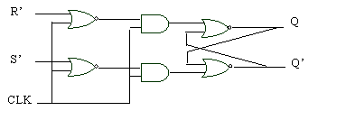
Schematic diagram of an edge-triggered flip-flop
Problem #3
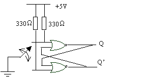 Debouncing
switch
Problem #4
|
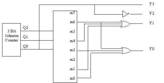
Q2Q1Q0 |
Decoder output that is 1 |
Y3 Y2 Y1 Y0 |
|
0 0 0 |
m0 |
0 1 0 1 |
|
1 0 0 |
m4 |
0 1 1 0 |
|
1 1 0 |
m6 |
0 1 1 1 |
|
1 1 1 |
m7 |
1 0 0 0 |
|
0 1 1 |
m3 |
1 0 0 1 |
|
0 0 1 |
m1 |
1 0 10 |
| Y3 = m7 + m3 + m1 = Q0
Y2 = m0 + m4 + m6 = Q0’ Y1 = m4 + m6 + m1 Y0 = m0 + m6 + m3 |