I. A sequential machine outputs a 1 when the input sequence x(t
- 2, t)=101 or 010, otherwise the output is 0.
(1). Draw the state diagram and write the state table.
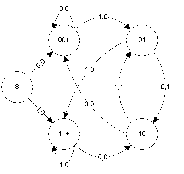
| Current State | Input x=0
Next State, Output
| Input x=1
Next State, Output
|
|---|
| S | 00+, 0
| 11+, 0 |
| 00+ | 00+, 0
| 01, 0 |
| 11+ | 10, 0
| 11+, 0 |
| 01 | 010, 1
| 11+, 0 |
| 10 | 00+, 0
| 101, 1 |
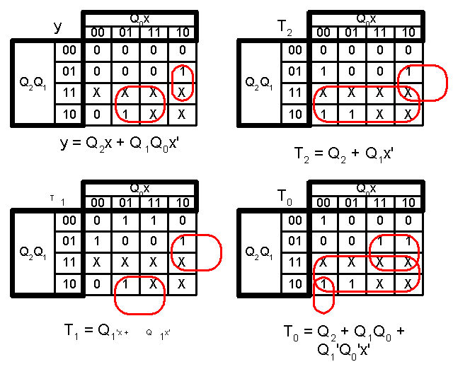
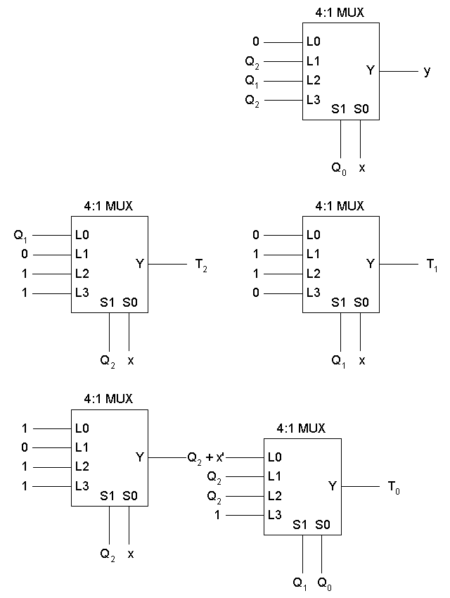
(2). Design the system with 3 T flipflops and a minimal
number of 4input multiplexers.
State Mapping
| State Mapping
|
|---|
| State Name | Q2
| Q1 | Q0
|
|---|
| S | 0
| 0 | 0
|
| 00+ | 0
| 0 | 1
|
| 11+ | 0
| 1 | 0
|
| 01 | 0
| 1 | 1
|
| 10 | 1
| 0 | 0
|
Transition Table
| Current State
| Input |
| Next State
| Output |
| Flip-Flop
Input
|
|---|
| Q2 | Q1
| Q0 | x
| | Q2
| Q1 | Q0
| y |
| T2 | T1
| T0 |
|---|
| 0 | 0
| 0 | 0
| | 0 | 0
| 1 | 0
| | 0 | 0
| 1 |
| 0 | 0
| 0 | 1
| | 0 | 1
| 0 | 0
| | 0 | 1
| 0 |
| 0 | 0
| 1 | 0
| | 0 | 0
| 1 | 0
| | 0 | 0
| 0 |
| 0 | 0
| 1 | 1
| | 0 | 1
| 1 | 0
| | 0 | 1
| 0 |
| 0 | 1
| 0 | 0
| | 1 | 0
| 0 | 0
| | 1 | 1
| 0 |
| 0 | 1
| 0 | 1
| | 0 | 1
| 0 | 0
| | 0 | 0
| 0 |
| 0 | 1
| 1 | 0
| | 1 | 0
| 0 | 1
| | 1 | 1
| 1 |
| 0 | 1
| 1 | 1
| | 0 | 1
| 0 | 0
| | 0 | 0
| 1 |
| 1 | 0
| 0 | 0
| | 0 | 0
| 1 | 0
| | 1 | 0
| 1 |
| 1 | 0
| 0 | 1
| | 0 | 1
| 1 | 1
| | 1 | 1
| 1 |
| 1 | 0
| 1 | 0
| | X | X
| X | X
| | X | X
| X |
| 1 | 0
| 1 | 1
| | X | X
| X | X
| | X | X
| X |
| 1 | 1
| 0 | 0
| | X | X
| X | X
| | X | X
| X |
| 1 | 1
| 0 | 1
| | X | X
| X | X
| | X | X
| X |
| 1 | 1
| 1 | 0
| | X | X
| X | X
| | X | X
| X |
| 1 | 1
| 1 | 1
| | X | X
| X | X
| | X | X
| X |
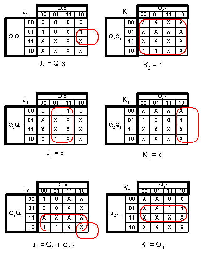
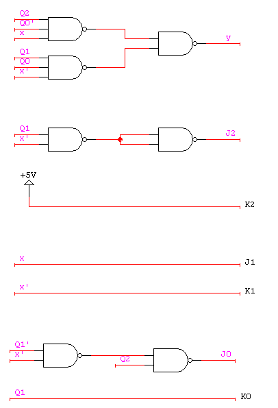
(3). Design the system with 3 JK flipflops and a minimal
twolevel NAND network.
| Current State
| Input |
| Next State
| Output |
| Flip-Flop
Input
|
|---|
| Q2 | Q1
| Q0 | x
| | Q2
| Q1 | Q0
| y |
| J2K2 | J1K1
| J0K0 |
|---|
| 0 | 0
| 0 | 0
| | 0 | 0
| 1 | 0
| | 0 X |
0 X | 1 X
|
| 0 | 0
| 0 | 1
| | 0 | 1
| 0 | 0
| | 0 X |
1 X | 0 X
|
| 0 | 0
| 1 | 0
| | 0 | 0
| 1 | 0
| | 0 X |
0 X | X 0
|
| 0 | 0
| 1 | 1
| | 0 | 1
| 1 | 0
| | 0 X |
1 X | X 0
|
| 0 | 1
| 0 | 0
| | 1 | 0
| 0 | 0
| | 1 X |
X 1 | 0 X
|
| 0 | 1
| 0 | 1
| | 0 | 1
| 0 | 0
| | 0 X |
X 0 | 0 X
|
| 0 | 1
| 1 | 0
| | 1 | 0
| 0 | 1
| | 1 X |
X 1 | X 1
|
| 0 | 1
| 1 | 1
| | 0 | 1
| 0 | 0
| | 0 X |
X 0 | X 1
|
| 1 | 0
| 0 | 0
| | 0 | 0
| 1 | 0
| | X 1 |
0 X | 1 X
|
| 1 | 0
| 0 | 1
| | 0 | 1
| 1 | 1
| | X 1 |
1 X | 1 X
|
| 1 | 0
| 1 | 0
| | X | X
| X | X
| | X X |
X X | X X
|
| 1 | 0
| 1 | 1
| | X | X
| X | X
| | X X |
X X | X X
|
| 1 | 1
| 0 | 0
| | X | X
| X | X
| | X X |
X X | X X
|
| 1 | 1
| 0 | 1
| | X | X
| X | X
| | X X |
X X | X X
|
| 1 | 1
| 1 | 0
| | X | X
| X | X
| | X X |
X X | X X
|
| 1 | 1
| 1 | 1
| | X | X
| X | X
| | X X |
X X | X X
|
II. Given a state table:
| NS, z
|
|---|
| PS State | x=0
| x=1 |
|---|
| A | B,1
| H,1 |
| B | F,1
| D,1 |
| C | D,0
| E,1 |
| D | C,0
| F,1 |
| E | D,1
| C,1 |
| F | C,1
| C,1 |
| G | C,1
| D,1 |
| H | C,0
| A,1 |
(1). Reduce the state table to a minimum number of states.
Combine those states with a common output pattern z. S1 = {A,B,E,F,G},
S2 = {C,D,H}
| NS, z
|
|---|
| PS State | x=0
| x=1 |
|---|
| A | B (S1)
| H (S2) |
| B | F (S1)
| D (S2) |
| C | D (S2)
| E (S1) |
| D | C (S2)
| F (S1) |
| E | D (S2)
| C (S2) |
| F | C (S2)
| C (S2) |
| G | C (S2)
| D (S2) |
| H | C (S2)
| A (S1) |
Separate those states with different transitions states. S3 =
{A,B}, S4 = {E,F,G}, S5 = {C,D,H}
| NS, z
|
|---|
| PS State | x=0
| x=1 |
|---|
| A | B (S3)
| H (S5) |
| B | F (S4)
| D (S5) |
| C | D (S5)
| E (S4) |
| D | C (S5)
| F (S4) |
| E | D (S5)
| C (S5) |
| F | C (S5)
| C (S5) |
| G | C (S5)
| D (S5) |
| H | C (S5)
| A (S3) |
Separate those states with different transition states again.
S6 = {A}, S7 = {B}, S8 = {E,F,G}, S9 = {C,D}, S10 = {H}
| NS, z
|
|---|
| PS State | x=0
| x=1 |
|---|
| A | B (S7)
| H (S10) |
| B | F (S8)
| D (S9) |
| C | D (S9)
| E (S8) |
| D | C (S9)
| F (S8) |
| E | D (S9)
| C (S9) |
| F | C (S9)
| C (S9) |
| G | C (S9)
| D (S9) |
| H | C (S9)
| A (S6) |
No more contradictions. Final states:
| NS, z
|
|---|
| PS State | x=0
| x=1 |
|---|
| S6 | S7, 1
| S10, 1 |
| S7 | S8, 1
| S9, 1 |
| S8 | S9, 1
| S9, 1 |
| S9 | S9, 0
| S8, 1 |
| S10 | S9, 0
| S6, 1 |
(2). Find a minimum length input sequence which will distinguish
between states A and B in the original table. Write the corresponding
output sequences with respect to an initial state A, and with
respect to an initial state B, respectively.
Two items to note:
- The outputs of A,B,E,F,G differ from the outputs of C,D,H
from the first state partitioning.
- A and B were split because A went to state S3 on a 0 when
B went to state S4 on a 0.
We must therefore look at S3 and S4 to see where they split into
either ABEFG or CDH at which point the outputs will differ. S4
immediately transitions to S5 on a 0 while S3 goes either to S3
or S4 on a 0. Once in S3/S4 and S5 a 0 differentiates the two
outputs. Therefore the shortest input string that differentiates
A and B is 000.
| State Sequence on Input 000 | Output
|
| ABFC | 111 |
| BFCD | 110 |
III. Given a modulo16 counter
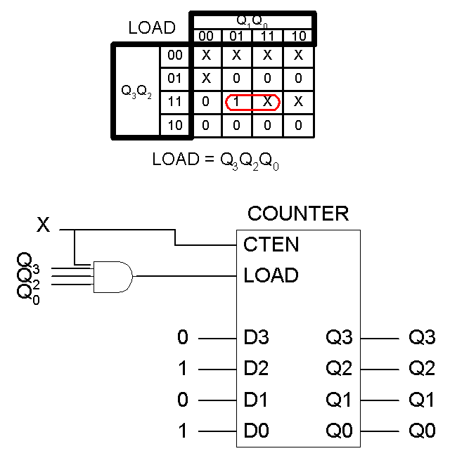
(1). Design a 5to13 counter with a minimal ANDORNOT
network.
Current State
Q3Q2Q1Q0
| Counter Input
D3D2D1D0
| LOAD |
|---|
| 0000 | XXXX
| X |
| 0001 | XXXX
| X |
| 0010 | XXXX
| X |
| 0011 | XXXX
| X |
| 0100 | XXXX
| X |
| 0101 | XXXX
| 0 |
| 0110 | XXXX
| 0 |
| 0111 | XXXX
| 0 |
| 1000 | XXXX
| 0 |
| 1001 | XXXX
| 0 |
| 1010 | XXXX
| 0 |
| 1011 | XXXX
| 0 |
| 1100 | XXXX
| 0 |
| 1101 | 0101
| 1 |
| 1110 | XXXX
| X |
| 1111 | XXXX
| X |
Clearly D3D2D1D0
= 0101.
(2). Design a counter with output sequence 9, 10, 11, 2, 3, 4,
7, 5, 12, 13, 15, 0, 1, with a minimal number of 2input
multiplexers.
Current State
Q3Q2Q1Q0
| Counter Input
D3D2D1D0
| LOAD |
|---|
| 0000 | X
| X | X
| X | 0
|
| 0001 | 1
| 0 | 0
| 1 | 1
|
| 0010 | X
| X | X
| X | 0
|
| 0011 | X
| X | X
| X | 0
|
| 0100 | 0
| 1 | 1
| 1 | 1
|
| 0101 | 1
| 1 | 0
| 0 | 1
|
| 0110 | X
| X | X
| X | X
|
| 0111 | 0
| 1 | 0
| 1 | 1
|
| 1000 | X
| X | X
| X | X
|
| 1001 | X
| X | X
| X | 0
|
| 1010 | X
| X | X
| X | 0
|
| 1011 | 0
| 0 | 1
| 0 | 1
|
| 1100 | X
| X | X
| X | 0
|
| 1101 | 1
| 1 | 1
| 1 | 1
|
| 1110 | X
| X | X
| X | X
|
| 1111 | X
| X | X
| X | 0
|


(3). Design a modulo64 counter with a modulo16 counter,
two SR flipflops and a minimal network of AND, OR, NOT gates.
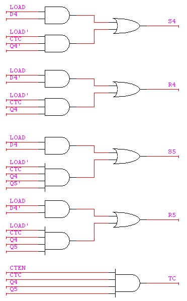
The schematic will look as follows. We must determine S5, R5,
S4, R4, and TC in terms of CTEN, LOAD, D5, D4, CTC.

Since TC follows CTEN (when CTEN is low, TC is low) we can use
it instead of CTEN.
| Current State
| | Next State
| | |
|---|
| LOAD | D4
| TC | Q4
| | Q4
| S4 | R4
|
|---|
| 0 | 0
| 0 | 0
| | 0 | 0
| X |
| 0 | 0
| 0 | 1
| | 1 | X
| 0 |
| 0 | 1
| 1 | 0
| | 1 | 1
| 0 |
| 0 | 1
| 1 | 1
| | 0 | 0
| 1 |
| 0 | 0
| 0 | 0
| | 0 | 0
| X |
| 0 | 0
| 0 | 1
| | 1 | X
| 0 |
| 0 | 1
| 1 | 0
| | 1 | 1
| 0 |
| 0 | 1
| 1 | 1
| | 0 | 0
| 1 |
| 1 | 0
| 0 | 0
| | 0 | 0
| X |
| 1 | 0
| 0 | 1
| | 0 | 0
| 1 |
| 1 | 0
| 1 | 0
| | 0 | 0
| X |
| 1 | 0
| 1 | 1
| | 0 | 0
| 1 |
| 1 | 1
| 0 | 0
| | 1 | 1
| 0 |
| 1 | 1
| 0 | 1
| | 1 | X
| 0 |
| 1 | 1
| 1 | 0
| | 1 | 1
| 0 |
| 1 | 1
| 1 | 1
| | 1 | X
| 0 |
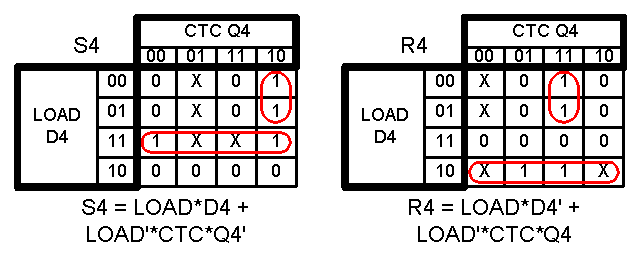
S5 and R5 are the same with the replacement of (CTC*Q4) for CTC:
S5 = LOAD*D5 + LOAD'*CTC*Q4*Q5' and R5 = LOAD*D5' + LOAD'*CTC*Q4*Q5.
TC is just the terminal count so it goes high when CTEN is high
and CTC and Q4 and Q5 are all 1's: TC = CTEN*CTC*Q4*Q5.
IV. Adder:
(1). A 2bit adder inputs (a1, a0,
b1, b0, cin) and outputs (cout,
s1, s0). Describe its truth table.
| a1 | a0
| b1 | b0
| cin |
| cout | s1
| s0 |
|---|
| 0 | 0
| 0 | 0
| 0 | | 0
| 0 | 0
|
| 0 | 0
| 0 | 0
| 1 | | 0
| 0 | 1
|
| 0 | 0
| 0 | 1
| 0 | | 0
| 0 | 1
|
| 0 | 0
| 0 | 1
| 1 | | 0
| 1 | 0
|
| 0 | 0
| 1 | 0
| 0 | | 0
| 1 | 0
|
| 0 | 0
| 1 | 0
| 1 | | 0
| 1 | 1
|
| 0 | 0
| 1 | 1
| 0 | | 0
| 1 | 1
|
| 0 | 0
| 1 | 1
| 1 | | 1
| 0 | 0
|
| 0 | 1
| 0 | 0
| 0 | | 0
| 0 | 1
|
| 0 | 1
| 0 | 0
| 1 | | 0
| 1 | 0
|
| 0 | 1
| 0 | 1
| 0 | | 0
| 1 | 0
|
| 0 | 1
| 0 | 1
| 1 | | 0
| 1 | 1
|
| 0 | 1
| 1 | 0
| 0 | | 0
| 1 | 1
|
| 0 | 1
| 1 | 0
| 1 | | 1
| 0 | 0
|
| 0 | 1
| 1 | 1
| 0 | | 1
| 0 | 0
|
| 0 | 1
| 1 | 1
| 1 | | 1
| 0 | 1
|
| 1 | 0
| 0 | 0
| 0 | | 0
| 1 | 0
|
| 1 | 0
| 0 | 0
| 1 | | 0
| 1 | 1
|
| 1 | 0
| 0 | 1
| 0 | | 0
| 1 | 1
|
| 1 | 0
| 0 | 1
| 1 | | 1
| 0 | 0
|
| 1 | 0
| 1 | 0
| 0 | | 1
| 0 | 0
|
| 1 | 0
| 1 | 0
| 1 | | 1
| 0 | 1
|
| 1 | 0
| 1 | 1
| 0 | | 1
| 0 | 1
|
| 1 | 0
| 1 | 1
| 1 | | 1
| 1 | 0
|
| 1 | 1
| 0 | 0
| 0 | | 0
| 1 | 1
|
| 1 | 1
| 0 | 0
| 1 | | 1
| 0 | 0
|
| 1 | 1
| 0 | 1
| 0 | | 1
| 0 | 0
|
| 1 | 1
| 0 | 1
| 1 | | 1
| 0 | 1
|
| 1 | 1
| 1 | 0
| 0 | | 1
| 0 | 1
|
| 1 | 1
| 1 | 0
| 1 | | 1
| 1 | 0
|
| 1 | 1
| 1 | 1
| 0 | | 1
| 1 | 0
|
| 1 | 1
| 1 | 1
| 1 | | 1
| 1 | 1
|
(2). Design a 2bit adder with a minimal twolevel NAND
network.
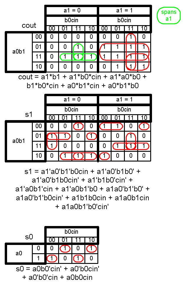
The NAND implementation is left to the student, -Craig
(3). Design a serial adder with a JK flipflop
and a minimal network of AND, OR, NOT gates.
(Doing this in HTML has worn me out. Please don't ask me to do
this one too -Craig)
V. System Designs:
Implement the following algorithm:
Alg:
{
Input
- X<0:7>, Y<0:7> type bitvector,
s-type boolean;
Localobject
- A<0:7>, B<0:7> type bitvector;
Output
}
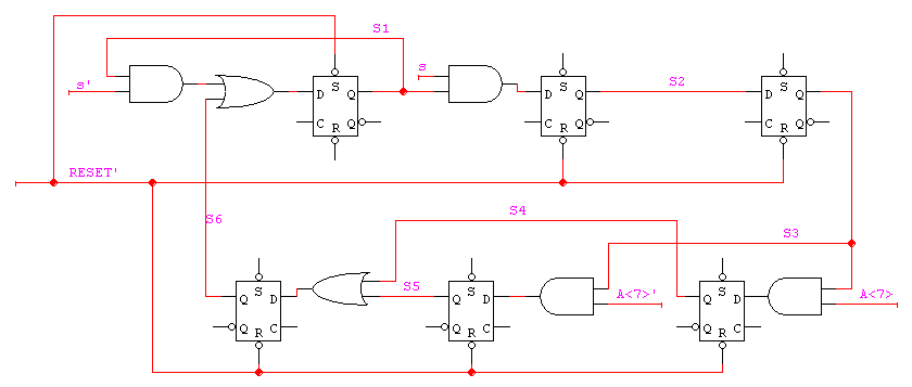
S1: if s' goto S1 else goto S2;
S2: B<X || A<Y;
S3: A<Add(A,B) || if A<7> goto S4 else goto S5;
S4: A<Add(A,1) || goto S6;
S5: B< Add(B,1);
S6: C< Add(A,B) || goto S1;
end Alg
(1). Design a data subsystem that is adequate to execute the algorithm
and draw the schematic diagram.
Data subsystem will require:
- A register
- B register
- Adder
- Mux for B or 1 input to Adder
- Mux for A or 1 input to Adder
- C register
- signal A<7> to control subsystem
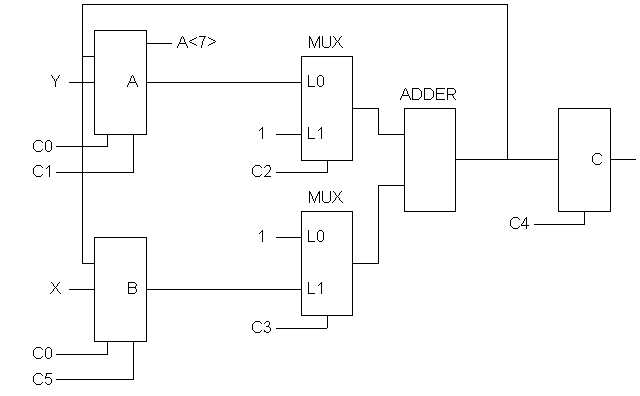
Control signals:
- C0: load A with Y and B with X
- C1: load A with Adder output
- C2: 0 selects A as Adder input, 1 selects "1" as
Adder input
- C3: 0 selects "1" as Adder input, 1 selects B as
Adder input
- C4: load C with Adder output
- C5: load B with Adder output
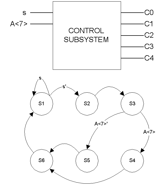
(2). Design a control subsystem and draw the state diagram.
| C0
| C1 | C2
| C3 | C4
| C5 |
|---|
| S1 | 0
| 0 | 0
| 0 | 0
| 0 |
|---|
| S2 | 1
| 0 | 0
| 0 | 0
| 0 |
|---|
| S3 | 0
| 1 | 0
| 1 | 0
| 0 |
|---|
| S4 | 0
| 1 | 0
| 0 | 0
| 0 |
|---|
| S5 | 0
| 0 | 1
| 1 | 0
| 1 |
|---|
| S6 | 0
| 0 | 0
| 1 | 1
| 0 |
|---|
- C0 = S2
- C1 = S3 + S4
- C2 = S5
- C3 = S3 + S5 + S6
- C4 = S6
- C5 = S5
(3). Implement the control subsystem with a one hot encoding design.
Draw the logic diagram.