cse141L
Lab
4:
Design Your Own ISA
Changelog
| February 13 |
Changed 'mem[pc]' to '&(mem[pc]);' in SuperGarbage.
|
| February 9 |
The late due date is 11:59pm on Sunday the 10th. There is no penalty for turning in lab 4 late. There will be a penality for turnining in lab 5 late.
|
| February 3 |
Some clarifications to the "Feasibility Issue" section. -jra
|
Due: 11:59pm, February 10
A Letter from Jake
| From: | Jake Ivring; CTO
|
UnicationITY, Inc. |
| To: |
Cob Bolwell; Principle
|
FlexGermanica Technical, LLC. |
Dear Cob,
Our revenues are getting hit by the knock-off clones from our low-cost rival, Boatorola Corp. The business strategist from Underson Consulting says our only hope for survival is to patent every aspect of our product. However, since many of the components are standard, there is nothing to patent. We need to redesign each piece so that it explores non-standard parts of the design space, which being new, will give our patent attorneys fodder for patent filings. Then when Boatorola copies us, we litigate for patent infringement!
We are hoping that you can pull together a team that can provide us with a new instruction set architecture that looks novel enough that we will have ample material to patent. We suggest as a start that you use a 17-bit fixed instruction size and 34-bit word size; that combination may help you explore a new design space. Furthermore, Boatorola has access to the MIPS and SPARC patent portfolio, so try not to be too similar to them. Of course, our products still need to be competitive, so the ISA should be general purpose and reasonably efficient. Also, since the fuse is relatively short on this, you will need to keep it simple. Your compensation will be based on the correctness, novelty and efficiency of the end product.
Thanks in advance,
Jake
Overview
As you read in Jake's letter, you should save your company by designing a novel processor in one month. In lab 4 and lab 5, you will focus on the design of your own ISA. This lab will not require the use of the Xilinx tools. Your ISA should be general enough to run all the provided benchmark programs, while being simple enough to allow you to implement a reasonably fast processor in the allotted time frame. Starting from lab 6, you will implement a working processor based on the ISA you design in lab 4.
Goals
Ultimately your ISA and resulting implementation will be evaluated according to the following criteria:
- General purpose
Is it able to execute the provided benchmark programs, and other general purpose programs?
- Novelty
How much is it different from existing ISAs such as MIPS or SPARC?
- Performance
How long does it take to run benchmark programs on your processor?
Requirements
Your ISA should fulfill the following requirements.
- Instruction width: 17 bit
- Data and address widths(word size): 34 bit
- General purpose enough to be able to run provided benchmarks and more general programs
- Include the following two instructions
- in [dest] [channel[3:0]] : read a 34-bit data from the specified channel and save at [dest]
- out [src] [channel[3:0]] : write a 34-bit data from [src] to the specified channel
- You must leave opcode space for expansion in case you leave out an instruction you need!
I/O (Input/Output) Instructions
Your ISA should support two I/O instructions - in and out. These instructions allow a processor to communicate with the external world via 16 channels. The width of a channel is 34-bit. The in instruction reads a 34bit data from a specified channel while the out instruction writes a 34-bit data to a specified channel.
I/O instructions have blocking semantics. If there is no data available to read by the in instruction, the processor simply waits until there is available data. Similarly, upon an out instruction, the processor must wait until the write operation completes; it might need to wait for available buffer space. You can freely use channels for various purposes such as debugging and multicore interface.
Benchmarks
Three benchmarks are provided to help guide your ISA development. In lab 4, you will write assembly programs based on your ISA for all three benchmarks. Assume that all the addresses (pointers) and data in the benchmark programs are 34 bit.
Program Loader
// function loader:
//    load a program in the data memory into the specified address of
//    the instruction memory
//
// src:  source address of the program in the data memory
// dest: destination address of the program in the instruction memory
// size: number of instructions to load, assume an even number
// part0(dptr *src):return 17-bit of the 34-bit data at src
// part1(dptr *src):return the remaining 17-bit of the 34-bit data at src
//
// note: this program does not need to run fast; but it does need to run.
//       dptr means data pointer which points to a 34-bit data,
//       while iptr means instruction pointer which points to a 17-bit instruction.
//       Since a data is 34-bit and an instruction is 17-bit, one data location contains
//       two instructions; part0 and part1 returns one of the two instructions, respectively.

void loader(dptr *src, iptr *dest, int size)
{
    int i
    for (i = 0; i < size; i+=2)
    {
        *dest++ = part0(src);
        *dest++ = part1(src);
        src++;
    }
    return;
}
SuperGarbage
// function supergarbage:
//    perform various operations
//
// opcodes
// 0: subtract
// 1: right shift
// 2: nor
// 3: swap
// 4: in
// 5: out
// 6: conditional jump with link
// 7: halt
//
// note: int is 34 bits

struct inst {
  int op;
  int srcA;
  int srcB;
  int dest;
};

int SuperGarbage(int pc, int *mem)
{
 while(1)
 {
  struct inst *instruction = &(mem[pc]);
  int op = instruction->op;
  int srcA = instruction->srcA;
  int srcB = instruction->srcB;
  int dest = instruction->dest;
  pc = pc + 4;

  switch(op) {
   case 0: mem[dest] = mem[srcA] - mem[srcB]; break;
   case 1: mem[dest] = mem[srcA] >> 1; break;
   case 2: mem[dest] = ~(mem[srcA] | mem[srcB]); break;
   case 3: temp = mem[srcB]; mem[dest] = mem[mem[srcA]]; mem[mem[srcA]] = temp; break;
   case 4: in  mem[dest], mem[srcA]; break; // in  mem, channel #
   case 5: out mem[srcA], mem[srcB]; break; // out data, channel#
   case 6:
     mem[dest] = pc;
     if (mem[srcA] < 0)
     {
      pc = mem[srcB];
     }
     break;
   case 7: return pc;
  }
 }
}
Fibonacci Number
// Recursive Fibonacci
//  get 'n'th fibonacci number
// You should not alter the algorithm

int fib(int n)
{
  if (n < 0)
    return 0x3DEADBEEF;
  else if (n <= 2)
    return 1;
  else if (n == 29)
    return 514229;
  else if (n == 30)
    return 832030;
  else if (n == 48)
    return 4807526976;
  else if (n == 49)
    return 7778742049;
  else return fib(n-1) + fib(n-2);
}
Feasibility & Implementation Issues
After this lab, you will be implementing your ISA in a Xilinx FPGA. If you are unfamiliar with these, please skim a Xilinx manual or talk with the TAs.
Xilinx makes a range of devices, from small to huge, but the free WebPACK we use can only synthesize to the smaller devices in each product line. (They want you to buy Foundation to use the biggest devices). We recommend targetting the Virtex-4 XC4VLX25.
You can look for
the Xilinx
product tables to get a rough idea of how big a design these parts can
hold. A logic cell is roughly equivalent to a gate. In any event, you should
keep your design to well under 10,000 flip flops, and under 15,000 logic
gates. So, for instance, a 32-element 16-bit register file is likely to have
at least 32x16 = 512 flip-flops, and probably at least one gate per flip flop
to control it. Keep these sizes in mind when deciding how many architectural
registers to provide in your ISA.
The instruction and data memories will be mapped to separate block-rams which
are available on the Xilinx part. These will be between 2 and 100 kilobytes,
however you should not assume anything about their size. These memories are
much smaller than the 34 bit address space your processor should be able to
support. Make sure your ISA design can support an instruction and data
address space of the full 34-bit range. Overly small address spaces is the #1
reason ISA's fail!
The latest Xilinx parts include large-scale logic blocks built into the chip that designers can use to improve their designs; for example, the XC4VLX25 has the equivalent of 48 multipliers. These are fair game for you to use in your design, if you find you need them. Check the Xilinx docs for more info on using them (both the WebPACK help files and datasheets on the Xilinx website).
Please don't use the embedded PowerPC processors available on some FPGA devices.
Useful Resources
| Deliverable |
Your team needs to submit a report, which should contain the following items.
- The name of your ISA and detailed explanation (two pages or so) of your design decisions.
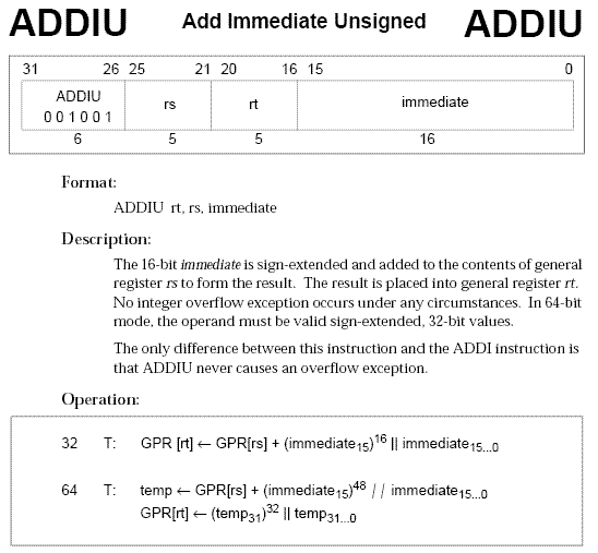
- Instruction manual with instruction names, instruction formats, and RTL descriptions of functionality. It should also include opcode maps, as explained in the class. For the manual style, follow the figure below, which is drawn from the MIPS R4400 manual. However, it does not need to be so ornately typeset.
- A description of all architectural (i.e. programmer visible) state (registers, stacks, memories, queues, etc)
- Stack management and function call / parameter passing conventions
- The three benchmark programs written in your ISA assembly language with heavy comments
|
Due: 11:59pm, February 10 |