
Introduction: This lab consists of two parts. In the first part you will be implementing the control unit for the divider, whose datapath was implemented in the second lab. In the second part, you will be implementing three Finite State Machines (FSMs) and comparing the results while using various kinds of Flip Flops and encodings.
| Cycle | CLR | End | LoadA | LoadQM | ShiftA | ShiftQ | Source | Q | A/S | SO |
| 0 | 1 | 0 | 0 | 0 | 0 | 0 | 0 | 0 | 1 | 0 |
| 1 | 0 | 0 | 1 | 1 | 0 | 0 | 0 | 0 | 1 | 0 |
| 2,5,8,11,14,17,20 | 0 | 0 | 0 | 0 | 0 | 0 | 1 | 1/0 | 1 | 1/0 |
| 3,6,9,12,15,18,21 | 0 | 0 | 1/0 | 0 | 0 | 0 | 1 | 1/0 | 1 | 1/0 |
| 4,7,10,13,16,19,22 | 0 | 0 | 0 | 0 | 1 | 1 | 1 | 1/0 | 1 | 1/0 |
| 23 | 0 | 0 | 0 | 0 | 0 | 0 | 1 | 1/0 | 1 | 1/0 |
| 24 | 0 | 0 | 1/0 | 0 | 0 | 0 | 1 | 1/0 | 1 | 1/0 |
| 25 | 0 | 0 | 0 | 0 | 0 | 1 | 1 | 1/0 | 1 | 1/0 |
| 26 | 0 | 1 | 0 | 0 | 0 | 0 | 0 | 0 | 1 | 0 |

The state diagram has nine states. The first state, S0, is the state where the circuit waits for the Begin signal. In this state all registers will be continuously cleared. On a clock signal the machine will move into state S1 where it will load the values for the divisor and dividend into the Q, M, and A registers. On the next clock signal the machine will enter the loop of states S2, S3, and S4.
During state S2, the subtraction will be allowed to occur. During state S3 the result of the subtraction will or will not be loaded back into the A register, depending on whether or not the result of the subtraction was positive. In state S4, the A and Q registers will shift. If the internal counter has reached 7 (the loop has completed 7 times), the machine will transition from state S4 to state S5. If not, then it will transition back to S2.
States S5, S6, and S7 are the same as S2, S3, S4 except for the fact that in state S7, The A register is not shifted. State S8 is the End state.
There are some state transitions which are not shown in this current state diagram. Independent of the current state, when you assert a low Begin signal, the next state must be S0. In order to be able to simplify the design procedure, you can derive your next state equations without considering the Begin signal and then connecting the Begin signal to the reset inputs of the flip-flops. This way you will need to worry about one less signal when you derive your state equations.
Note: the above implementation is not the most efficient, nor the only correct solution. You may implement any state based controller, so long as it correctly controls the given divider circuit.
You are supposed to design the controller as a state-based design. The overall structure of your controller design should look like the one in the following figure:

In order to be able to implement the controller, you need to follow the steps given below.
Simulate your circuit with the following data:
110100100011001 / 11110010
We provide you our version of the division circuit here (right click, save as...).

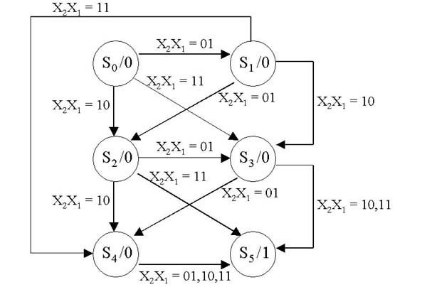
You should first implement this machine using D flip-flops, then using T flip-flops. Which implementation is better from an area point of view? Why?

Since we have 6 states, we need 3 bits to encode each of them. You should to use the following codes:
| State | Output | 1st case | 2nd case |
| S0 | 1 | 100 | 101 |
| S1 | 0 | 110 | 011 |
| S2 | 1 | 010 | 110 |
| S3 | 1 | 011 | 001 |
| S4 | 1 | 001 | 111 |
| S5 | 0 | 000 | 000 |
The first case minimizes the number of bits that change at each transition, while the second case maximizes it! You should first implement this machine using JK flip-flops, then using T flip-flops. Which implementation is better from an area point of view? Why? Remember to implement both encodings for both kinds of flip-flops.
Requirements:
For both parts of this experiment, pleasen turn in cost and performance analysis for each implementation
referring to the delay formulas in lab 4. For part one you should try your circuit
using the same examples that were given to you in the 2nd lab assignment, and
turn in the results for each simulated input. And, of course, you should
submit your circuit files, following the standard procedure.