cse141L
Lab
3:
TrivialScalar - Control
Changelog
| April 19 |
Added some clarifying information about the specific workings of the dmem and imem. A mini-section has been added that addresses
the communication protocol behind these two modules.
As a result of the above change, the state machine now has a new state (DMEM Read). More information is available in the
state machine image and in the table below it.
After some deliberation, we've decided that another (fairly simple) construct needs to be added to the Datapath that was
not explicitly mentioned in the last lab. This is described below in the "Datapath Addition" section. Hopefully this
change should make your lives much easier. This also includes a signal addition to the control module (named stall).
We've tried to mark all of the relevant changes in red text.
|
| April 20 |
Added a small change to the Datapath PDF which should fix a small bug manifested in the changes that were posted yesterday.
Also clarified the intended input placement of the instruction MUX on the Datapath PDF. Here's a summary:
-
A "0" input to the MUX should select the output coming directly from the
imem.
-
A "1" input to the MUX should select the output coming from the DFF between the
imem and the MUX.
Lastly, the inst control signal that was accidently erased in the last Datapath PDF change has been
added back.
|
| April 22 |
The due date for lab 3 has been shifted to April 29th.
A few design changes have been made to simplify (and clean up) the TrivialScalar design. The following changes
are the most notable:
-
The
imem is now an asynchronous ROM. A tutorial for generating this type of memory has been provided
in the Appendix at the bottom. As you scroll to it, please skim over the lab text for anything that you may have
missed or that we may have added.
-
In light of the above change, all of the newly added circuitry has been removed (including all of the intricate
DFFs and the MUX between the
imem and the decode modules).
-
The PC hardware no longer operates a cycle ahead of the rest of the processor. This should greatly
simplify how you and your team thinks about the processor's operation.
-
In light of the first change, the input and output stall signals have been removed from the datapath
and the control modules, respectively.
The design is very similar to its original incarnation, with just a few noted changes. We've attempted to make
those as apparent as possible throughout the body of the lab. I would suggest that the first thing that you do
from this point forward is to make your top-level design conform to the
new datapath.
|
Due: April 29
Overview
In Lab 3 you will extend the design demonstrated in Lab 2 to implement the control unit for TrivialScalar.
As you probably realized throughout Lab 2, it wasn't very easy to test each individual module completely;
however, with the addition of Lab 3 (the control unit), testing will be much more straightforward.
As in Lab 2, our aim for this lab is to help each of you to learn/master the skills necessary to succeed in the
coming labs. Please use one of the many resources you have available to you (the TAs, WebBoard, and your
classmates) if you become stuck.
NOTE: You must complete Lab 3 in the same groups you completed Lab 2 with.
Please remember that you must conform to the class
coding standards. They are
available here.
If you find a bug in them (e.g., they are causing you to do something horribly ugly), please let the professor
or one of the TAs know.
The greatest common divisor example is
available here. Create a
new project and import all the files. If you
simulate using gdb_tbw.tbw, it will run a short test.
This example demonstrates the coding standards for
the datapath and the modules therein.
Getting Started
General Notes
- As in Labs 1 and 2, "Virtex4 - XC4VLX15" will still be our target device.
-
This PDF details the datapath (for this lab) and the control signals (for Lab 3).
- All Verilog used in these labs should be synthesizable.
IO in TrivialScalar
Here are some notes about how IO should work in TrivialScalar. You should read through this before starting the implementation below.
Please note that all of the signals shown below (in the diagrams) should be held for an entire cycle.
On a READ instruction, in_req signal should be asserted for an entire cycle (as shown in the following figure) and the processor
should block for a response from the IO device. The IO device may take any number of cycles to respond to the request. However,
the earliest that the IO device may respond would be the following cycle. The figure below demonstrates the in_req
signal being asserted and the IO device responding in the third cycle following the initial request by placing data on the
in_data line and asserting the in_ack line for an entire cycle. The data on the in_data
line is only valid while the in_ack line is asserted.

WRITE instructions work similarly as the out_req signal is asserted while the data to be passed to the IO device is
placed on the out_data bus (as is shown in the following figure). The IO device may respond any number of cycles later
by asserting the out_ack wire. As in the case of a READ instruction, the earliest time for a response is the following
cycle. The figure below demonstrates the protocol for communicating with the IO device. On a WRITE instruction, the out_req signal
should be asserted while the data to be transferred to the IO device should be on the out_data bus. The processor must
stall until the IO device has completed the request (which is signaled by a cycle-long assertion of out_ack).

TrivialScalar's Dmem/Imem
Here is some insight as to how the memory modules work in TrivialScalar. Some more contextual information is available
in the table below.
Firstly, it is important to note that the dmem module in TrivialScalar is positive-edge triggered and that the imem
module is asynchronous. What this means to you, as the architect, is that a read or a write in the dmem can only occur at a
positive edge of the clock signal. All reads through the imem will still occur in a single cycle. The implications
of this are that a read on a memory location (in the dmem) require an entire cycle to show up on its output bus. The direct
impact of this observation is pointed out below and in the following section.
On an LD instruction, the following should take place: the read_write_req signal should be asserted, the proper input
to r_data should be selected via the reg_sel signal, and the regfile_write_en signal should be asserted
at the proper time. Know that an access to the dmem takes about a cycle, so the LD operation takes a total of two
cycles. This is part of the state machine design detailed in the next section, and is reiterated and emphasized throughout that section.
On a ST instruction, the protocol is more straight-forward. The following signals have specific importance during this
instruction: both read_write_req and dmem_write_en should be asserted in order for the dmem to latch
onto its inputs at st_data and addr. Although this operation takes time, just as the LD operation does,
since we've eliminated the extra propagation delay between dmem and the register file, we don't have to continue
for an extra cycle. The value should have been stored into the dmem by the following cycle.
Datapath Addition
In an effort to clean up the Datapath design, we ask that you please remove any additions from between the imem and the
decode modules.
Control Implementation
The main focus of this lab is creating a single module: control. We'll go ahead and call it control.v.
Control
The interface listed below lists each signal in the order it should be encountered while looking through the PDF schematic:
// Parameters:
//  INST_WIDTH -> Width of an instruction
module control#(parameter INST_WIDTH = 16)
(
	// Global clock
	input clk,
	// Global reset
	input reset,

	// Control-Datapath interface
	//  Specifies which PC should be used next cycle
	output [1:0] run_stall_reset,
	//  The entirety of the current instruction from the Decode unit
	input [INST_WIDTH - 1 : 0] inst,
	//  Write enable for the dmem
	output dmem_write_en,
	//  Request for a read or write from the dmem
	output read_write_req,
	//  Selects the data to be written to the register file
	output reg_sel,
	//  Write enable for the register file
	output regfile_write_en,
	//  Specifies the op code for the ALU unit
	output op_code,

	// The control interface for IO
	// More details to follow
	input in_ack,
	input out_ack,
	output out_req,
	output in_req
);
We'll be designing the control unit as a state machine. If this is unfamiliar to you, consult
Verilog Design Examples by Krste Asanovic. If the concept of state machines is still foreign, please talk to one of the TAs.

The above image shows the different states that the control module (and therefore the processor) can have. The below
table should explain the different states:
| State |
Meaning |
RUN |
This state is representative of the normal processor execution, where each PC should advance by one
each cycle. In this state, the processor is not looking for any particular signals from the outside
world. Be aware that this state will have to perform some preparation when moving from one state to the next (like
stalling the processor for a cycle).
|
DMEM Read |
Although we might like for a load from the dmem to take just a single cycle, it unfortunately must take longer than that
with a synchronous memory. The dmem takes about a cycle to fetch the data for a given input, which doesn't leave enough
time for the fetched data to propagate to the register file. Knowing this, we must wait an extra cycle on each LD instruction in order
to account for dmem latency and general propagation delay. The processor will effectively be stalled here, as in the other states,
however, we already know that it must resume the following cycle (so we aren't waiting on a response). The challenge in this case
will be asserting the proper signls at the correct time in order to avoid latching on to the wrong data.
|
IO Write |
This state is in effect when the control module encounters a WRITE instruction. The processor
should be completely stalled while in this state, waiting for a cycle-long out_ack (but not in_ack!). During
the first cycle of the WRITE instruction, the control module should (as demonstrated in the IO section above)
assert the out_req output to "pass" the value on out_data to the IO device (this should happen
in preparation for this state--see the note in the RUN state). Note that the datapath
handles the placement of the data in R1 on the out_data bus.
|
IO Read |
This state is similar to the IO Write state except that it stalls waiting for a cycle-long
in_ack, and it asserts the in_req output on a READ instruction in order
to request for data to be placed on the in_data bus. The control module must
also route the proper data (in_data) to the Register File. (As in the IO Write case,
be aware of the note about performing preparation in the RUN entry above).
|
HALT |
This state just signifies when the processor has seen a HALT instruction. The processor should stall indefinitely
from this point on, until it is reset.
|
Updated:
It is important to note the many different ways that this state machine can be designed. For more information on our requirements
for the design of this state machine, consult the document from last lab:
Verilog Design Examples by Krste Asanovic.
What I'm referencing here is the state machine design detailed throughout the above PDF. Your control module should be similar
in concept to the GCD state machine (expect somewhat more complicated). Don't forget to use only three always blocks,
initialize your signals on every cycle to avoid repeated statements, and to comply with the class Verilog coding standards throughout
the design process.
Below are some tips for the generation of each signal. I won't give away much information, but just enough to get you started.
run_stall_reset
The run_stall_reset signal will be choosing which of the three signals will propagate to become the Next PC.
This signal might be particularly tricky because the diagram isnt entirely specific of what inputs to the mux generate which outputs.
To be more specific, the ordering of the signals entering the PC MUX shouldn't matter in terms of design rules. If you or your group
feels that you can generate a more efficient control implementation by switching around which signal enters which terminal of the MUX,
please go ahead and do so. Your implementation must continue to adhere to the other aspects of the specified design. Be aware that
this signal (among others) depends greatly on instruction being executed and the next_state the control unit will enter into.
Updated:
On another note, be aware that your reset signals should be asynchronous throughout the "stateful" parts of your processor. This
allows for your always blocks to trigger on the edge of a reset signal instead of relying on your reset signal to stay
high until a positive clock edge is generated.
Question 1: Make a table of all of the control signals that are generated by the Control unit and specify if each signal
depends on the state of the processor, doesn't depend on the state of the processor, or a little of both.
dmem_write_en
This signal should just be asserted when it is time to write to the dmem.
read_write_req
This signal should just specify when there is either a read or a write occuring at the dmem.
reg_sel
This signal is similar to the read_stall_reset signal in that it chooses from multiple inputs through the use of a MUX.
In this case, it is also recommended that you choose an optimal ordering for the MUX inputs that simplifies your Control code.
regfile_write_en
This is just the write enable for the register file. Beware that for one particular instruction, when you assert this signal will
be crucial for proper operation of the instruction/processor.
Question 2: Which instruction is referenced at the end of the last paragraph and why would we not want to assert it immediately?
op_code
This signal should just specify which operation we would like to execute in the ALU.
in_ack, out_ack, in_req, and out_req
Please refer to the IO explanation above for the operation of these signals.
TrivialScalar High-level Implementation
Now that we have all the individual pieces designed and functioning, we can go ahead and put together our processor. We'd like
to make a high-level file called processor.v and instantiate and connect our two large modules together. Here's the interface
for that:
module processor
(
	// Global clock
	input clk,
	// Global reset
	input reset,

	// The data interface for IO
	input [7:0] in_data,
	output [7:0] out_data,

	// The control interface for IO
	input in_ack,
	input out_ack,
	output out_req,
	output in_req
);
Test Benches
Using Test Benches and *.coe files
For starters, go ahead and test your TrivialScalar implementation with the provided test program and testbench.
Here's a link to a test program in (*.coe) format that you can use to verify
your processor implementation. This should just be attached to your imem module, just as the
memory generation tutorial specifies. You can change the properties of a generated memory by double clicking
on the module (imem in this case) and bringing up the Block Memory Generator. On
page 3 of 4, you'll have the option of changing the init file (*.coe file). This is where you'll want
to specify this new file.
Question 3: Provide a translation of the provided *.coe file into assembly.
In addition to this file, you'll need to stimulate the inputs specific to this *.coe file (speaking in terms of
the IO module). Here's a *.zip which contains the test bench files that you can use in conjunction with the above
test.coe file.
Question 4: How many cycles after the first IO-based instruction does the IO device respond.
Please provide a screenshot of a waveform describing this.
Generating/Writing Test Benches
After using the provided *.coe file and test bench above, we'd like you to generate your own set of testing tools.
We would like each group to write up a test program that takes two inputs from the IO module, operates on them,
and then sends them back down the IO path. Assuming the two inputs are X and Y (received in that order from the IO
unit) function we'd like you to perform is ((X + Y) * Y - 3). We'd like for you to do this three times
in your code (remember that this ISA doesn't have a branch--so no loops!), writing back your result to the IO device
after each computation. Please generate your own test bench that provides your processor with the proper IO responses.
I would recommend variation in the delay of the IO responses so that each of the three iterations have some differences
in timing, as this is most likely how we'll be testing this.
Note that this set of test bench will test your IO instructions, but you'll have to verify visually that your protocol
matches the one listed in this write up (since this test bench cannot examine and report on the protocol itself).
Question 5: As described in the paragraph above, create your own *.coe file with the above parameters and
test bench waveform (*.tbw--and its counterpart *.tfw file) file to accompany it. Feel free
to use a more loosely timed clock for this portion (although your propagation time shouldn't be
above 10ns, ideally). Provide both the contents of the *.coe file
and the assembly you derived it from.
Performance Evaluation
Now that your processor should be completely working (and these results will really only be valid in such a case),
you should go ahead and perform some performance-based analysis on your design. You should use the static timing
report generation tool to accomplish this. You will need to change a few settings in order to get the results that
are required of you:
-
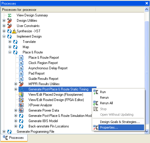
Go ahead and select your top-level module in the Sources pane and right click on Implement Design->Place and Route->
Generate Post-Place & Route Static Timing. Select properties.
-
Select Advanced as the Property Display Level. Make sure that Report Type is set to
Verbose Report and that Perform Advanced Analysis is checked. This will show much more detail
in the report.

Question 6: Go ahead and implement your design and generate the above mentioned timing report. What is
the maximum achievable frequency of your design? (Hint: The critical path is the path with
the longest delay. Shortening this path increases your maximum frequency.) Describe your
critical path through the circuit (e.g. PC_Mux->PC_DFF->etc...).
General Tips
-
Before starting post-route simulations, be sure that you've exhausted your options with a behavioral simulation.
Behavioral simulations are much faster and much less resource intensive, and thus you'll get your results faster.
-
Note that your generated test benches are very hackable, as they are completely human-readable. Just open up a
*.tfw file and take a look. The "$monitor" and "$display" keywords may be of interest. The following
primer may be of interest.
-
Create
localparams to represent different states and typical inputs/outputs, so that your code
isn't inundated with 4'b000, 4'b0001, etc. with no specific meaning tied in with those values (this is similar
to using enums or #defines in C/C++).
Appendix
Generating Distributed (Asynchronous) Memories [imem]
NOTE: The Xilinx Core Generator may not function correctly in Linux. Our experiences have yielded errors late in the generation verison.
You can either brave it in Linux, or you can use the Windows version (in the lab, if need be). If you've had success with the Core
Generator in Linux, please let one of the TAs know.
-
In the ISE viewer go to "Project"->"New Source". Select "IP (CORE Generator & Architecture Wizard)" on the left. Decide on a
file name for the particular component you're designing and type it into the "File name" field. The naming scheme in the screenshot
below demonstrates a <memory type>_mem_<width>_<size> scheme. Click next at this point.

-
In the "Memories & Storage Elements"->"RAMs & ROMs" folder, choose "Distributed Memory Generator", click next, and the finish.

-
- Enter your desired depth into the "Depth" field (I would recommend something small--around 128, unless your really need a ROM of that size).
- Enter 16 as your "Data Width" (the width of an instruction).
- Select the "ROM" radio button and then click next.

-
Click browse and locate your desired coefficients (*.coe) file to preload the ROM with. Be sure that the "Default Data" box reads 0.
Nothing else should be set here. Go ahead and click finish.

-
The memory module will take around 10-15 minutes to be generated. Watch the console for its progress.
For usage instructions, please consult the *.veo file (one is generated for each module), which should
now be located in your project directory. Or, if you just want the module's inputs and outputs, highlight
the newly generated module and, in the processes tab, navagate to "CORE Generator"->"View HDL Functional Model".
Look for the "module" declaration directly under the "timescale" statement.
| Deliverable |
- Submit your report for the questions above to both TAs (to reduce the risk of a lost or bounced email) via e-mail by the due date before the beginning of the class.
- Answer all of the questions (6) found in the lab description.
- The report should be in a single PDF file (including answers to questions, verilog source code, graphs, screenshots, etc).
There are many tools out there capable of integrating text and graphics and producing PDF files (OpenOffice does a pretty good job).
- Please include your zipped project directory in your email. Your project directory should include all of your project files,
including all of the test bench and *.coe files mentioned in this lab. Please use the following naming convention:
cse141L-lab1-LastName1-FirstName1-LastName2-FirstName2-LastName3-FirstName3.zip with your group members' last names and first names
substituted for LastName1-3 and FirstName1-3, respectively.
- Name your PDF file cse141L-lab1-LastName1-FirstName1-LastName2-FirstName2-LastName3-FirstName3.pdf with your group members' last names
and first names substituted for LastName1-3 and FirstName1-3, respectively.
- The subject line of your email should read "[CSE141L] Lab 3 Submission - LastName1, FirstName1 - LastName2, FirstName2 - LastName3, FirstName3".
|
Due: April 29 |