CSE 140L Lab 2 - Sequential Circuit Design
Spring 2009, Professor Cheng, TAs Thomas Weng, Renshen Wang, Chengmo Yang, Mingjing Chen
Due time: Demonstrate by 5/5 11:59PM, Report by 5/5 11:59.
Important! Please regularily check http://webboard.ucsd.edu for the latest updates and news regarding this lab. FAQs and announcements will be on the webboard, so check it often!
Objective
- Learn how to use flip-flops.
- Learn how to design basic sequential circuits like shifters, counters, etc.
- Learn how to use the FPGA board to demonstrate your sequential circuits.
- Learn how to design a working clock using flip-flops.
We will give you guys a tutorial on a very basic sequential circuit. Here you will learn how to use the
on-board clock. Also, we will provide a step-by-step instructions for using
the VHDL editor and creating modules with it. We will also provide the VHDL code to use.
IMPORTANT: thoughout all the parts of this lab, the clock frequency will be 1 Hz.
For parts 1 and 2, pressing the left button will start the cycle, while pressing the right button will reset/clear the cycle.
For parts 3, 4, and 5, pressing (and holding down) the left button will accelerate the
clock by 10 times (hint: consider the 2-to-1
MUX you built in Lab 1), while pressing the right button should reset the circuit.
The rest of the lab will not contain as detailed instructions. However, we will give hints as needed.
Importamt - For the timing and functional outputs, we want the
actual output, NOT the segment display output. So similar to lab 1,
please use output ports before the segment display modules like you did
for the adder and mux.
Part 0. Sequential Circuit Tutorial
For this part, you will simply follow the tutorial to learn some of the basics that you will need for this lab.
Lab 2 Tutorial
Part 1. 8-bit Shift Register
For part 1, you will be designing an 8-bit shift register using D
flip-flops. To demonstrate this on the board,
you will be designing your shifter so that you shift the red line on
your LED outputs. Normally your board will display nothing, but when
you press the left button (you will have to hold it down for a second
or so), you send an input of 1 into the first flip flop, which causes a
red line to be shifted every second around the segment display. The
output pattern will look like:
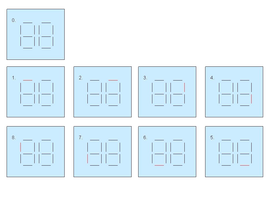
Use the tutorial as a starting point for this circuit.
Configure your D flip-flops in such a way that you capture this
shifting. The left button will be used to start the cycle, and the
right button will be used to clear all the segment displays. Note: You can ignore the
leftmost two LED displays (just use HEX0 and HEX1).
Report:
- Include schematic diagrams of your circuit
- Include functional and timing diagrams of your simulation. (10 clock cycles will do, as your shifter will have repated).
- Include functional and timing diagrams of your simulation when you press the reset button
- Explain what happens in your functional simuation when you press the reset button. What happens to all the outputs?
- Explain why this shifter is "sequential" as opposed to the combinational circuits you did in lab 1.
What does sequential even mean?
- Draw out what the outputs would look like if you tied a "1" into the first flip flop (draw out 10 cycles).
Part 2. Johnson Counter
You will design an 8-bit Johnson counter in this part of the lab.
The 8-bit output will be mapped to LED using the same way as part 1. The
right button will be used to reset your counter.
Report:
- Include schematic diagrams of your circuit
- Include functional and timing diagrams of your simulation.
- Explain how a Johnson Counter is similar and different from your 8-bit shift register.
Part 3. Asynchronous Counter
In this part, you will build an 8-bit asynchronous counter using T flip-flops. You will output the results
on the segment display. The left number will display the MSB, and the right one will display the LSB. Therefore
your pattern will look like: 00, 01, 02, 03, ... 0F, 10, 11, ... , F0, F1, ... FF. Therefore you will need two
4-bit binary display modules to output the corrent number on the segment display.
We provide you the VHDL code DEC_7SEG.vhd
for the two LED digits for you to use. Implement this the same way as
the tutorial demonstrated. You will also need to learn how to use bus
inputs for this part. The left button will speed up the clock 10x as
mentioned above, and the right will reset.
Report:
- Include schematic diagrams of your circuit
- Include functional and timing diagrams of your simulation.
- Explain why this is an asynchronous counter, as opposed to your synchronous shift register.
- Write one to two paragraphs explaining how an asynchronous
counter works. Convince us you know how and why the numbers get counted
up every cycle.
- When the initial clock cycle of the first FF is too small, the "clk"
input of the following FF cannot hold stably. In your simulation, try
to change the initial clock frequency to make the counter fail.
Simulate this test bench and mark the time point where the counter
fails in simulation waveforms. Explain why it fails.
Part 4. Pseudo Random Sequencer
Design a 4-bit pseudo random sequencer to display a random
number on the segment display using ONLY four D flip-flops and a 2-input XNOR gate.
The initial value is "0000". Your design target is to maximize the
period of the pseudo random sequence generated by the circuit.
You will display a random number in digit 0. The left button will speed
up the clock 10x as mentioned above, and the right will reset.
Report:
- Include schematic diagrams of your circuit
- Include functional and timing diagrams of your simulation.
- What does it mean "pseudo" random? Why is this not a totally random sequencer?
Part 5. Clock
In this part, you will design a clock. Your clock will count up
from 0 to 59, and then back to 0. So the sequence will be 00, 01, ...
09, 10, 11, ... 58, 59, 00, etc. You will need to learn how to reset
the counter properly to get correct carries. The left button will speed
up the clock 10x as mentioned above, and the right will reset.
Report:
- Include schematic diagram of your circuit
- Include timing simulation diagrams of your simulation. (Functional not
necessary, good if you make it)
- Explain how you designed your circuit to handle the carries and reset properly.
Demonstration
You will need to demonstrate your project to a lab TA. Please
look at the office hours for when we are available. Note, you can
contact us if those times do not work, as we are happy to meet you outside
those times too durning the evening. For your demonstration, you will
need to demonstrate part 4 and 5. You can bring your laptop with your
FPGA board to us and program the FPGA board in between demonstrations.
So you will first program your board with Part 4, and demonstrate your pseudo random sequencer,
and then reprogram it with your Part 5. For those of you without a laptop, we will
try to set up machines in the lab that have Quartus II for your use, so you can
bring your saved files on a flash drive or email and reprogram on the lab machines.
If all looks good, we
will give you thumbs up. If something doesn't work correctly, then
please go back and fix it.
Report Instructions
You lab report should include:
- Title page, which contains Names and PID of students, due date,
title of lab, and brief discription of each person's contribution.
- Part 1 - schematic diagrams, functional diagrams, timing diagrams, and answers
- Part 2 - schematic diagrams, functional diagrams, timing diagrams, and answers
- Part 3 - schematic diagrams, functional diagrams, timing diagrams, and answers
- Part 4 - schematic diagrams, functional diagrams, timing diagrams, and answers
- Part 5 - schematic diagrams, timing diagrams, and answers
Grading
30% of your grade will be from the demonstration, so this is an
easy 30%. Another 40% will be in your logic schematics and timing
diagrams. Easy points assuming you were able to demonstrate this for
us. 30% will be in your answers to the questions.