Project Homework #2
Due: Monday, May 12, 1:00 PM
In this part of the project, you are asked to implement a
placement algorithm that is a hybrid of slicing bisection and simulated
annealing based approaches for an N-row
style standard-cell design.
Overview:
This part of the
project aims at specifying the concrete positions of the components in an N-row standard-cell design. As you have
learned in the course, one important issue for standard cell layout is how to
reduce the number of feed-throughs that connect non-adjacent rows. The slicing
bisection algorithm could be an appropriate technique for attaining this goal,
as we discussed in class. To optimize the circuit delay, the components in each
row should be arranged in such a manner that the overall interconnect length
within each channel is minimized. Therefore, the placement tool you will be
implementing in this part consists of two major steps. In the first step, the
components need to be grouped into distinct rows using the slicing bisection algorithm.
The concrete position of each component in its corresponding row is
subsequently determined in the second step using a simulated annealing based
algorithm.
Row-based
Component Grouping:
In this phase, the
components of the circuit are grouped into N-different
rows using the slicing bisection algorithm. Initially, the algorithm generates
a suitable partitioning between the first row (a slicing) and the remaining N-1 rows. Then in the set of components
corresponding to the remaining N-1
rows, a further partitioning between the second row and the remaining N-2 rows is generated. This process is
repeated till each component is assigned to a row. In each partitioning step,
the algorithm aims at minimizing the cutsize between the two partitions so as
to reduce the difficulty in the subsequent routing phase. As you might have
already observed, such a slicing process can be implemented by repeatedly
performing a Fiduccia-Mattheyses type of partitioning algorithm that you
already implemented in the first part of the project. However, due to the
particularity of the slicing problem, several small modifications need to be
performed as described below.
Feed-through
Reduction: The slicing bisection algorithm performs partitioning in a gradually
reduced set of components. However, in order to reduce the number of
feed-throughs, it is necessary to keep track of the connections between the
components currently being partitioned and the components in the rows already
fixed. More specifically, if a component has strong connections with the
previously generated rows, it will be a better choice to assign this component
in the top row of the current sub-partitioning. This necessitates the
implementation of a terminal propagation scheme to help ensure the
feed-throughs are minimized. In the following part of the writeup, we will
suggest to you two ideas that may help you achieve this goal.
(1)
In each partitioning step, instead of performing a
partitioning on the set of components that have not yet been assigned to a
certain row, apply the partitioning algorithm to the complete set of
components. However, the components that have already been assigned in previous
steps must be fixed in Partition 1
and are not allowed to move. Consequently, each partitioning step will generate
a partitioning between components that have been assigned (Partition 1) and the components yet to be assigned (Partition 2). The size of Partition 1 will be increased by the
size of a new row of components in each partitioning step. Such a strategy will
automatically assign the components that are heavily connected to the
previously generated rows into the new row being generated, thus reducing the
number of feed-throughs.
(2)
To further push the algorithm to avoid feed-throughs, we
can further penalize the moves that could generate feed-throughs. This is
accomplished by assigning a large penalty value P to the edges between the components that have already been
assigned and the ones yet to be assigned. The rationale for such a strategy
stems from the fact that if a component that heavily connects with the
previously generated rows is moved to Partition
2 (the case where a feed-through is generated), the cutsize will be
significantly increased.
Ratio of Partitioning: Since an identical row width is preferred in standard
cell design for area minimization, the slicing bisection algorithm begins from
a highly unbalanced partitioning, with the size of Partition 2 being nearly N-1
times of the size of Partition 1.
Each partitioning step will increase the size of Partition 1 by the size of one row and reduce the size of Partition 2 by the identical size. In
the last partitioning step, the size of Partition
1 becomes nearly N-1 times of the
size of Partition 2. Such a varying
size ratio requires you to update the area constraints of the
Fiduccia-Mattheyses algorithm in each step. More formally, in step m, the area constraints should be
specified as the following formula to reflect the fact that there are m rows in Partition 1 and N-m rows
in Partition 2.[*]
floor(m|V|/N - Cmax) <=
|Partition 1| <= ceiling(
m|V|/N + Cmax)
floor[(N-m)|V|/N - Cmax]
<= |Partition 2| <= ceiling[
(N-m)|V|/N + Cmax]
Slicing Bisection
Algorithm:
1.
Partitioning step 1: Generate an initial partitioning
between the first row and the remaining N-1 rows using the Fiduccia-Mattheyses
algorithm under the area constraints specified above.
2.
In partitioning step m,
fix the components assigned to the first m-1 rows in Partition 1, and
regenerate a partitioning of the complete set of components under the updated
area constraints as specified above. The penalty value P of the edge between components that have been assigned and
components yet to be assigned is used in the computation of the gain of each
tentative move.
3.
Repeat step 2 until every component has been assigned to
a certain row.
Intra-row
Component Arrangement:
Now you have already determined
the component assignment to each row. However, the concrete position of the
components in each row is still not yet specified. This task will be performed
by a simulated annealing algorithm that minimizes the overall interconnect
length. As you have learned in the course, achieving such an optimization goal
is crucial for reducing the delay of the circuit.
Algorithm Overview: The simulated annealing
algorithm mimics the annealing process. The algorithm starts from an initial
placement and iteratively adjusts the placement until little cost reduction can
be obtained in a prespecified number of successive iterations. The adjustment
of the placement is selected in a random manner. Adjustments that lead to cost
reduction are always accepted. However, the algorithm also probabilistically
accepts layout perturbations that increase the cost in order to climb out of
local optimum. The adjustment of a component position can only be performed
within each row so as to obey the results of the component assignment phase.
Cost Function Model: The simulated
annealing algorithm aims at reducing the overall interconnect length. Since the
detailed routing information is not yet available at the placement phase, the
cost is modeled as the total horizontal wire lengths which can be
accurately computed based on the placement. Moreover, only the interconnects
within each channel are estimated in the cost model, and the feed-through wires
are ignored. An example of wire length estimation is shown in Figure 1. The
total estimated wire length (only the horizontal wires) for this figure is 32.
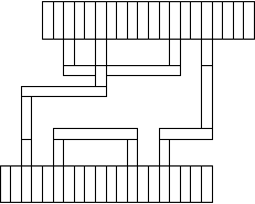
Figure 1 Wire length estimation
Pin Location Model: As you might have seen in Figure
1, the computation of horizontal wire lengths requires the specification of pin
locations in each row. The pin location specification is illustrated in Figure
2. This example shows a shape of a component with 3 pins. In this figure, the
parameter size is equal to the size of the component defined in the
first assignment, and the pin numbers correspond to the pin numbers given in
the circuit connectivity matrix. The pin numbers increase from left to right
starting with 1. The distance between two adjacent pins within the same
component is 2, and each pin is of width 1. Since the fabrication technique
targeted by this placement tool assigns a distinct metal layer for feed-through
wires, as we will see in the subsequent part of the project, you do not need to
consider the space of feed-through areas in each row. Consequently, the
adjacent components in each row are arranged closely.
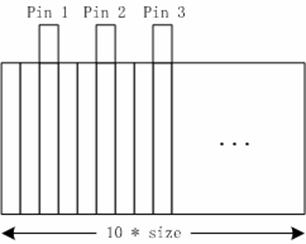
Figure 2 Pin location specification
Simulated Annealing
Algorithm:
1.
Create an initial placement by just using the initial
ordering of the components. Choose initial T
as the number of components in your circuits. The constant that is used to
modify the temperature should be chosen as 0.9.
2.
Choose a component randomly. The component can be chosen
from any of the rows. You might first choose the row randomly and then randomly
choose a component from that row. Then change the position of the selected
component to a random location in the same row. Changing the location may
entail pushing the intervening blocks appropriately. If a block is moved to the
right, intermediate blocks will be pushed left, and vice versa. The distance
calculations for the connections of all intervening blocks will be affected
consequently. Calculate the new estimated wire length. Naturally, if the wire
length is less than the initial wire length, the move is accepted. If the new
wire length is larger than the initial wire length, you calculate the quantity e-(new cost - old cost) / T.
This quantity must be between 0 and 1. At this point you pick a random number
between 0 and 1, and if the number that you have picked falls short of the
calculated quantity, you accept this move (i.e. you accept a "bad" move, thus
hoping to avoid a local minimum); otherwise this move is ignored.
3.
Repeat step 2 for a number of times before changing the
temperature. For a circuit with N
components, the number of moves tried at each temperature shold be (N*N)/2.
4.
Decrease the temperature by using the formula, Tn
= 0.9 * Tn-1. Then go to step 2. The algorithm should terminate when
the improvement between the successive iterations (outer-loop iterations, not
the inner-loop iterations at each temperature) falls short of 2% of the current
cost three times in a row.
Implementation:
The
number of rows, N, in the layout is
dependent on the number of components in the circuit. For your implementation,
specify N with the following
equation. This ensures that the layout will be in a near-square shape.
N = floor( )
)
The number
of feed-through wires in the layout highly depends on the penalty value P employed in the slicing bisection
algorithm. We provide to you a set of candidate P values, namely, {1, 2, 5, 10,
15}. You are asked to run your algorithm with these P values, and provide an empirical knowledge as to which P value is generally most effective in
terms of feed-through reduction.
Input Output Specification:
The input
specification of your program is exactly the same as the first assignment.
In the first phase:
-
Print out the best P value determined by empirical experiments.
-
Print out the current cutsize after each partitioning step with the algorithm running with the best P value.
-
At the end of the first phase, print out the component assignment results and the number of feed-through wires. For example:
Partition 1: 1 5 8
Partition 2: 0 2 4 6
Partition 3: 3 7 9
Number of feed-through wires: 2
In the second phase:
-
Calculate and print out the initial cost (total horizontal wire length required by this placement).
-
For each temperature, print out the current temperature and the final cost for that temperature.
-
When the algorithm terminates, print out the final placement together with the final estimation of the wire length.
Self-test Examples:
Here are the two different circuit connectivity matrices.
What to turn in:
1.
A file including your program together with the results
of your program for the two example circuits given in the writeup. Your program
output should follow the format specified above.
2.
A document detailing how you implement the algorithm in
your code. Provide a detailed analysis as to how you determine the best P value.
3.
Your program source code files and a README file that
explains how to compile and run your program.
Turn-in Method:
Send all requested files to the TA via email. The email must be
time-stamped by the deadline.