// D_WIDTH  : data width
// PA_WIDTH : port address width

module core#(parameter D_WIDTH = 34, PA_WIDTH = 4)
(
    input  clk,
    input  reset,

    // I/O interface
    output in_req,
    output out_req,
    output [PA_WIDTH-1 : 0] in_addr,
    output [PA_WIDTH-1 : 0] out_addr,
    input  [D_WIDTH-1 : 0]  in_data,
    output [D_WIDTH-1 : 0]  out_data,
    input  in_ack,
    input  out_ack
);
The core interface is simple - it consists of clk, synchronous reset, and I/O interface. When 'reset' signal transitions from high to low, the processor core starts executing from the 0x0 of the instruction memory. The I/O interface provides the interface for in and out instructions, which communicate to the outside world. Since the available pins are usually very limited, the I/O interface multiplexes 16 channels into one physical channel to save the pincount. All I/O interface signals are edge-triggered.
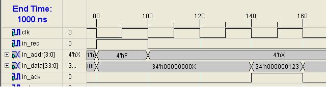
The I/O interface is similar to a conventional bus interface. 'in' instruction asserts 'in_req' and 'in_addr', then waits for 'in_ack' to become 1. If 'in_ack' arrives, the backend stores 'in_data' into the register the 'in' instruction specifies. In the best case, the 'in_ack' signal will arrive in the next cycle, but it can be arbitrarily delayed if no data is available in the specified channel. In the waveform example below, the core asserts 'in_req' with 'in_addr' to 0xF. The core spends two idle cycles, then it stores 0x123 to the register file when 'in_ack' signal arrives.
'out' instruction works in a similar way; but the backend also asserts 'out_data' along with 'out_req' and 'out_addr'. After asserting a request, the backend waits for 'out_ack' comes. Like 'in_ack', 'out_ack' could arrive after an arbitrarily long delay, signaling the completion of a request. In the waveform example below, the core asserts 'out_req' with 'out_addr' to 0xF and 'out_data' to 0x123, then waits for 'out_ack' comes. When 'out_ack' signal is asserted after one cycle, the core completes out instruction.

Q1. Review your fetch unit and update it if you need to. For each change you made, explain the reason in your hardcopy report. If you think your processor is fine with the existing fetch unit, you do not need to make any change.
A register file is essential to store register data of your processor. It should support read and write operations simultaneously, and have an interface along the following lines. (You may need to add more read/write ports.)
  // SEL_WIDTH : number of bits needed to specify a register
  // D_WIDTH : data width

  module regfile#(parameter SEL_WIDTH = 4, D_WIDTH = 34)
  (
	  input  clk,
	  input  we,
	  input  [SEL_WIDTH-1 : 0]  read_sel0,
	  input  [SEL_WIDTH-1 : 0]  read_sel1,
	  input  [SEL_WIDTH-1 : 0]  write_sel,
	  input  [D_WIDTH-1 : 0]    din,
	  output [D_WIDTH-1 : 0]    dout0,
	  output [D_WIDTH-1 : 0]    dout1,
  );

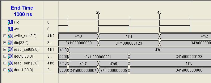
Note that writing a value to a register occurs at the clock edge, while reading a register does not involve any clock edge. In other words, 'we', 'write_sel', and 'dout' are edge-triggered, while 'read_sel0', 'read_sel1', 'dout0', 'dout1' are level-triggered as you see in the figure above. For example, if you assert 'we (write enable)' signal before the clock edge in a certain clock cycle with 'write_sel', 'din' will be stored in the specified register at the rising edge of the next clock. In contrast, if you change 'read_sel0' or 'read_sel1', 'dout0' or 'dout1' will be changed in the same clock cycle. Examine how a register file behaves in the following waveform. Note that the written value is updated at the clock edge, while 'dout0' and 'dout1' changes instantly when 'read_sel0' or 'read_sel1' changes. You might be able to implement a register file using flip-flops.
Your processor has two memory modules - an instruction memory and a data memory. While the instruction memory is a part of the fetch unit, the data memory is located in the backend. You should use the provided wrapper module for the data memory. Like the register file, it allows read and write operations, however it does not support simultaneous read and write in a clock cycle. In one cycle, the data memory can serve either a read operation or a write operation.
Memory Wrapper Module: dmem.v (will be posted soon)
   module dmem#(parameter A_WIDTH = 13, D_WIDTH = 34)
  (
          input  reset,
	  input  clk,
	  input  read_write_req,
	  input  write_en,
	  input  [A_WIDTH-1 : 0] addr,
	  input  [D_WIDTH-1 : 0] din,
	  output [D_WIDTH-1 : 0] dout,
	  output refused
  );
Data memory interface is straightforward. All the signals of the data memory module are edge-triggered, and you can assert the following signals for read and write operations.
Then, why do we need 'refused' signal? 'refused' signal indicates that the memory module cannot service the requested operation at that time. There are a few reasons for the asserted 'refused' signal; the memory could be being refreshed; or another processor core has already been using the memory in the multi-core system. Although 'refused' signal is not used in this lab, your backend must be able to tolerate the 'refused' signal; if 'refused' is asserted upon a memory request, the backend should request the same operation until it succeeds.

In the waveform above, the core requests one write operation and one read operation. Unfortunately, the data memory cannot service the read operation, asserting 'refused' signal. Upon the 'refused' signal, the core requests the same operation in the next clock and successfully get the memory value in the second trial.
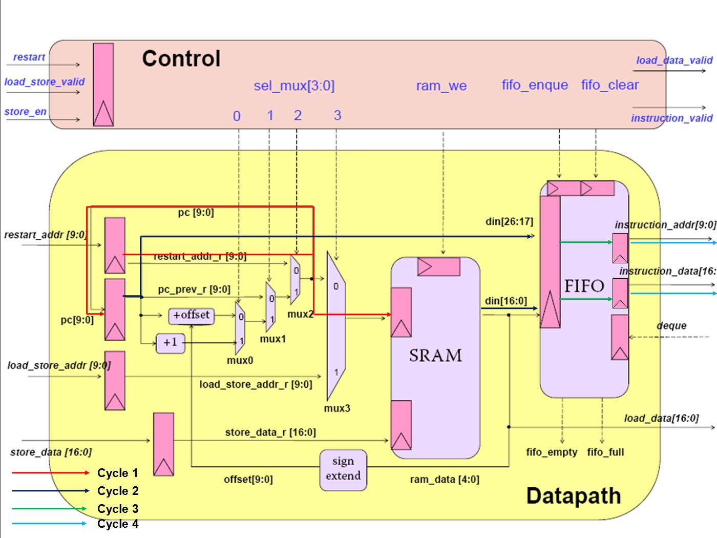
In addition to the register file and memory module, you would need other components in the datapath of the backend. In the case of the fetch unit, you used a few adders, a sign extender, and a few muxes to get the updated PC. For the backend, it depends on your ISA and how you implement it.
Q2. List all the other leaf modules needed for the backend of your processor. For each module, list all the instructions that use the module.
// I_WIDTH  : isntruction width
// IA_WIDTH : instruction address width
// D_WIDTH  : data width
// PA_WIDTH : port address width

module backend#(parameter I_WIDTH = 17, IA_WIDTH = 12, D_WIDTH = 34, PA_WIDTH = 4)
(
    input  clk,
    input  reset,

    // inputs from the fetch unit
    input  [I_WIDTH-1 : 0]  instruction_data,
    input  [IA_WIDTH-1 : 0] instruction_addr,
    input  instruction_valid,
    input  [I_WIDTH-1 : 0]  load_data,
    input  load_data_valid,

    // outputs to the fetch unit
    output deque,
    output restart,
    output [IA_WIDTH-1 : 0] restart_addr,
    output load_store_valid,
    output store_en,
    output [IA_WIDTH-1 : 0] load_store_addr,
    output [I_WIDTH-1 : 0]  store_data,

    // I/O interface
    output in_req,
    output out_req,
    output [PA_WIDTH-1 : 0] in_addr,
    output [PA_WIDTH-1 : 0] out_addr,
    input  [D_WIDTH-1 : 0]  in_data,
    output [D_WIDTH-1 : 0]  out_data,
    input  in_ack,
    input  out_ack
);
Roughly the interface of the backend consists of two parts - the fetch unit interface and the I/O interface. Both interfaces are already explained before.
For Q4 and Q5, answer questions with the style used in the following example.
Question: what happens when 'restart' and 'restart_addr' is asserted? assume that 'load_store_valid' is not asserted.
Answer: Assume that 'restart' and 'restart_addr' are asserted in cycle 0.
example answer schematic
Q6. Implement a register file module for the backend of your processor in RTL Verilog, and name the file regfile.v. Include the full source file in your hardcopy report.
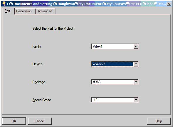
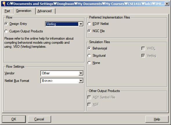
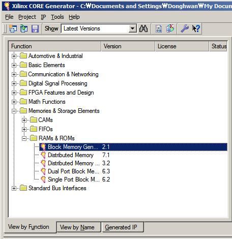
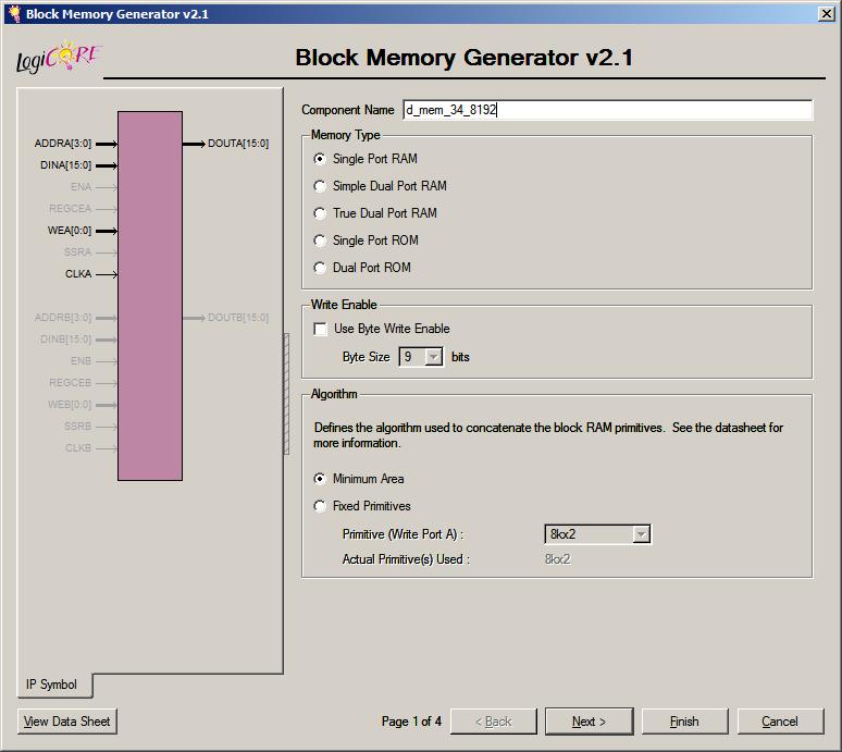
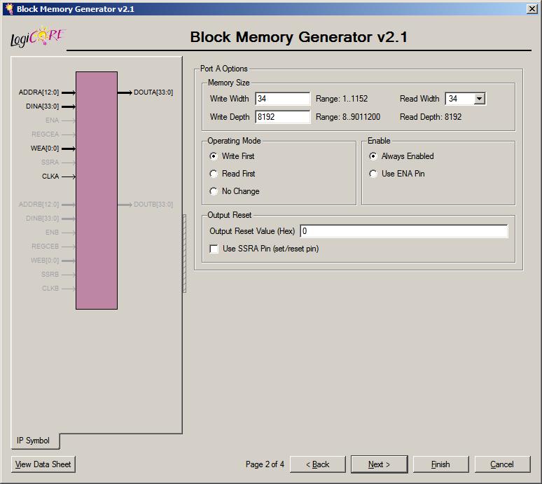
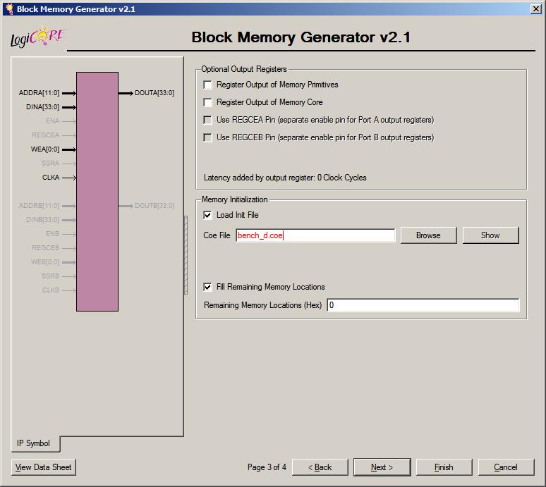
Q7. Unlike for the register file, it is better to use a highly optimized memory generator for the data memory module rather than writing your own data memory module. Fortunately, Xilinx provides a utility named CORE Generator for such a purpose. Gererate a 8K word size data memory module named 'dmem_34_8k' with CORE Generator. You can follow a step-by-step tutorial at the end of this page to do it. For the initialization of the memory module, use any coe file you generated in lab 2b. Write a testbench which tests whether your memory module is working correctly, and then actually test your memory module. Capture the behavioral simulation result screen and include it in your hardcopy report with explanation. The captured screen should clearly show 1) read and write operations work correctly, and 2) memory is properly initialized with the provided *.coe file. The generated module should be used with the provided wrapper module dmem.v.
Q8. Implement all the other modules required in your datapath. You have to implement each module in a separate .v file with RTL Verilog as you did for modules like adders, muxes, and sign extenders in lab 1. You might find that you can reuse many leaf modules used in the fetch unit. Also include full Verilog source code in your hardcopy report.
Q9. Implement 'backend.v' in structural Verilog for the backend of the processor. You can skip control logic in lab 3a. Since it is hard to test an implementation without control logic, it is enough to show that your Verilog file is synthesizable and implementable. You will complete the implementation with control logic in lab 3b.
Q10. Implement 'core.v' for the top module of the your design. You can simply wire up the fetch unit and the backend. No control logic required for 'core.v'.