CSE 140L Lab 2, Part 0
- Sequential Logic Lab Tutorial
Spring 2007, Professor Cheng, TAs Thomas Weng, Chengmo Yang, Yi Zhu
This tutorial will demonstrate how to construct an asynchronous 2-bit counter using Quartus II.
By following this tutorial, you should be able to know:
1. How to construct sequential logic circuits by using essential components such as clock sources, flip-flops, etc.
2. How to build a hierarchical block using VHDL source files instead of block diagrams.
3. How to specify bus input/output.
4. How to perform functional and timing simulation on sequential logic circuits.
In addition, there is a BUG in Quartus II when specifying the clock source input. You may follow this tutorial (step 6) to resolve this bug .
Build a 2-bit Asynchronous Counter
A 2-bit asynchronous counter, which is constructed by two T flip-flops, is shown in the following logic diagram:
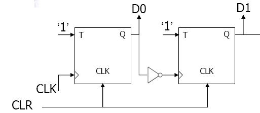
Now we implement this circuit in the board, such that it will count every second, use push button 2 to clear (reset), and display D1 and D0 on LED digit 1 and digit 2 respectively. The steps could be as follows:
1. Create a new project and a new block diagram file. Add two T flip-flops (in /primitives/storage/tff). Connect an input pin PB2 to the CLRN inputs of the two flip-flops and VCC to the two T inputs. Follow the diagram to connect the output of the first flip-flop and the clock input of the second one by adding an invertor between them. This is simple and straightforward.

2. Next we create the clock source. The board provides us a 25-MHz oscillator which can be used as a global clock input. However, we need some module to convert it to the 1-Hz clock. We provide the VHDL code CLK_DIV.vhd to serve this purpose. It can convert the 25-MHz clock to various other frequencies, from 1-MHz to 1-Hz. Now copy this file to your working directory and then create a hiearchical block called CLK_DIV. Double click the block, then it will automatically connect to the VHDL code.
3. Create an input to the CLK_DIV block and connect it to an input pin "clk"; create an output from the block to the first flip-flop. Specify the input and output of the block as well as the mapper properties. Note that the input port of the block is "clock_25Mhz" and the output port is "clock_1Hz". To get all the port names, check the "PORT" part in the file CLK_DIV.vhd (lines 8-17). For details about this procedure, check the previous tutorial. After this step, the diagram looks like the following.

4. Copy the file Binary_display.bdf to your working directory. Construct two hierarchical blocks for display and connect them to the outputs of two flip-flops respectively. You must be familiar with that already. However, instead of connecting 8 output pins to the hierarchical block directly, we connect one bus output to each block and name them as LSD[7..0] and MSD[7..0] respectively. Specify the mapping properties for each LSD[0] to LSD[7], MSD[0] to MSD[7] respectively, as shown in the following screen shot.

5. In other place of the diagram, create 8 output pins for each block. Each pin is connected to a wire, which is name as LSD[0], LSD[1], ... The Quartus II compiler will automatically connect them to the buses. Thus, it is important to keep the name consistency between buses and output wires.
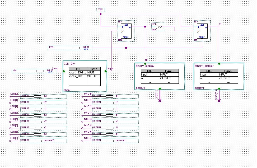
6. Specify pin numbers for each input and output. The input pin number for the clock is 91. However, you may get the following error message when trying to specify this pin. This should be a bug in Quartus II. We may tentatively specify it using another unused pin number (e.g. 41). After finishing the compilation, go to the Pin Planner and changet it to 91. Recompile the design, then we will get rid of this bug.

7. Now compile the design and download it to the board. You should be able to see the LED counts every second!
8. After testing the design on board, we can also perform functional and timing simulation. Since the clock frequency is 25MHz, and the time horizon in simulation is only 1 us, we do not need the CLK_DIV block to switch the frequency to 1 Hz. Therefore, throughout the simulation in Lab 2, we need to modify the diagram to bypass the CLK_DIV circuit. It is shown as follows.

9. Create an input wave form file and add 2 input pins clk and PB2 to it. Right click the clk pin, choose Value-Clock.. in the menu and specify the clock period as 40 ns or 25 MHz, as shown below. Also, right click the PB2 pin, choose Value-Forcing High (1), since we do not want to clear the counter.
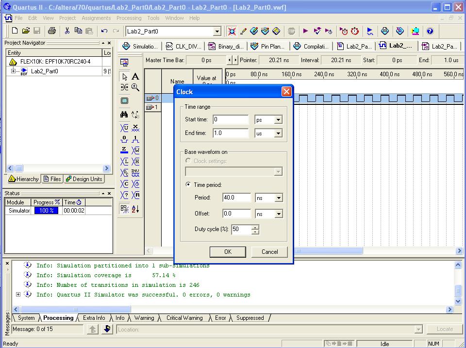
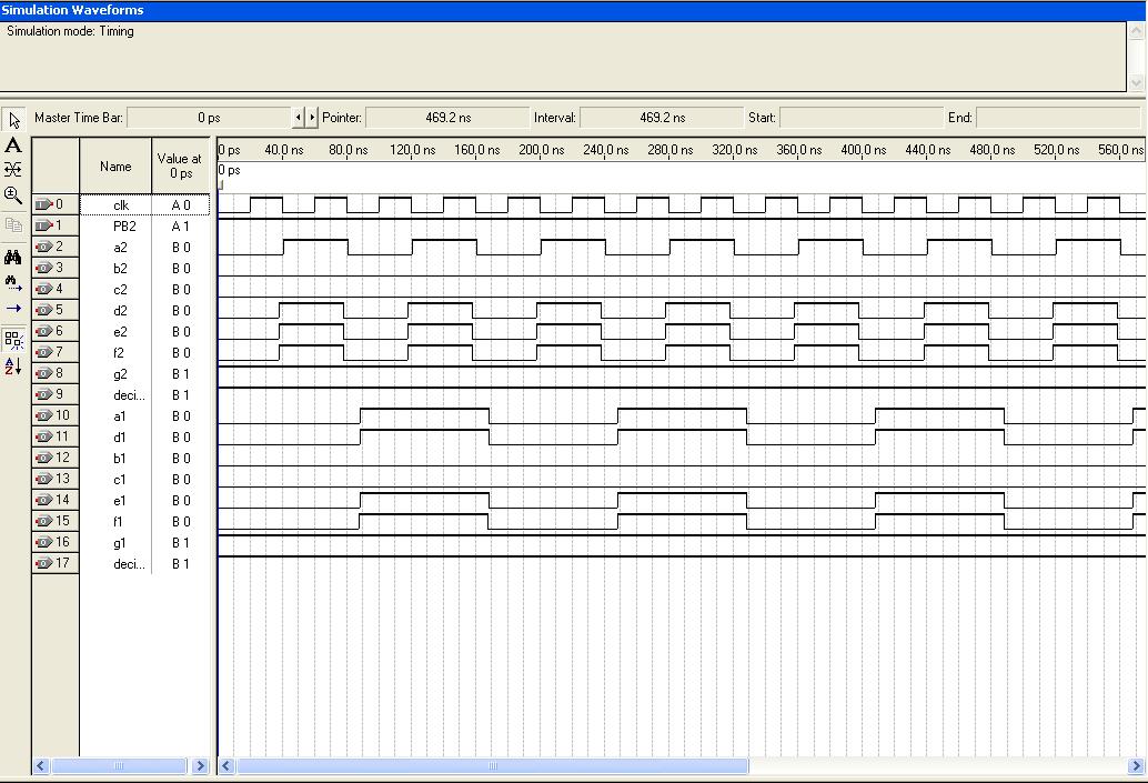
10. Perform the functional and timing simulation as Lab 1. You will obtain the following results.
Functional Simulation Results:
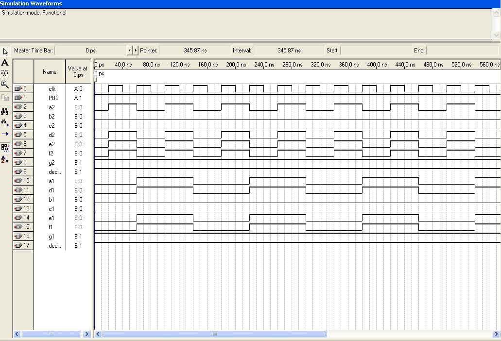
Timing Simulation Results: