CSE 140L Lab 1, Part 4 - Adder Tutorial
Spring 2007, Professor Cheng, TAs Thomas Weng, Chengmo Yang, Yi Zhu
In this part, you will design an full adder. You will learn how to create a module with a combinational circuit, and how to use that module in higher level circuits. By breaking up a combinational circuit into modules, you can begin to design more complicated circuits. You will use your 1-bit number displayer from part 3 to display the results on the segment display.
You will run your adder circuit on the FPGA board. The switches 1-3 will be used as inputs; and the two LED digits will be used to display the sum and carry out bits respectively. In our report, you will be required to include the logic diagrams as well as the simulation results.
Part 1. Build Hierarchical Blocks
First we will demostrate how to build a display module by using the logic diagram we built in Part 3 step by step. This is very important to build complciated circuits in later assignments.
1. Create a new project using "New Project Wizard" in Quartus. Open an empty block diagram file. Also copy the block diagram file in part 3 into your current project directory and rename it as "Binary_Display.bdf". Only keep the portion that displays the 0/1 on digit2.
2. In the empty block diagram file, choose "block tool" icon (as highlighted by the red circle in the following screens shot) and then use your mouse to drag a block in the schematic window. Change the block name as "Binary_Display" (this name must match the name of your .bdf file) and the instance name as "display1". Double-click the block you can view the block diagram built in part 3.

3. Right-click the block, choose "Block Properties" in the menu and then "I/O" tab, add the input and output ports you want to have for this block. Here we have only 1 input which is the bit we want to display, and 8 outputs which are the 7 segments in LED and one decimal point. The port names must be matched with the names of input and output ports in the block diagram file Binary_Display.bdf.

4. Create 1 input pin and 8 output pins. Assign switch 1 to input pin and the LED digit 2 (including the decimal point) to output pins in Pin Planner respectively. Save your design.
5. Connect these pins to the block. Change the type of each wire from "Conduit Line" to "Node Line" by right clicking on the wire segment.

6. Double click each joint point of the wire and the block (as highlighted); in the "Mapper Properties" pop-up window, choose "Mappings" tab, enter the fields of "I/O on block" and "Signals in node". The name of the first field must match the corresponding port name in Binary_Display.bdf; the name of the second can be arbitrary and will be the name of the connected wire.
IMPORTANT: You may change the wire name later or the wire has been assigned a name before connection. Make sure that the second field matches the wire name all the time, otherwise you will get compilation error. To change the wire name, right click the wire and then choose "Properties".

7. Compile your design and download it to the board. You would get the same result on digit2 as part 3. However, you have built the hiearchical block "Binary_Display" for further use. You can easily copy this block and change the input/output pins to display other information on both digits!
Part 2. Create a Half Adder
A half adder has only two inputs: addends A and B, and also produces two outputs: sum S and carry-out Cout. The truth table of a half adder has been given in CSE140 class. The logical expressions of S and Cout can are as follows:
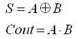
Create a logic diagram with two gates to build a half adder. Display carry-out Cout and sum S on digit1 and digit2 respectively, using the Binary_Display block built above. You need to copy the block and change the input and output pins accordingly.
Part 3. Create a Full Adder from Half Adders
A full adder has three inputs: two attends A and B, a carry-in Cin. The adder adds up the three inputs, and generates a sum bit S and a carry-out Cout. The truth table is also given in class. We can deduce the logic expressions of S and Cout as follows:
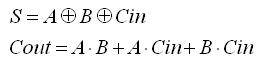
To understand how we can build the full adder from half adders, one remembers that the two addends A, B, carry-in Cin as well as the sum S are of weight 1, while the carry-out Cout is of weight 2. We first use a half adder to add up A and B, generating an intermediate sum S_int and an intermediate carry-out Cout_int1. We then use another half adder to add up the intermediate sum S_int and the carry in Cin, producing the final sum S and another intermediate carry-out Cout_int2. Cout_int1 and Cout_int2 can never be both 1 (could you answer why?), hence are ORed together to generate the final carry-out Cout. The logic expression for Cout can be rewritten as:

Such a design is pictured in the following figure.
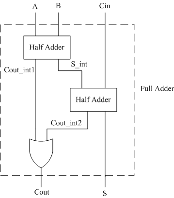
Hence, to build a full adder, first use the logic diagram you created for a half adder as a block, then follow the above diagram to construct the full adder. Compile your design and test it on board. Also perform the funtional and timing simulation, as taught in part 1.