CSE 140L Lab 1, Part 1 - Basic Combinational Circuit Tutorial
Spring 2007, Professor Cheng, TAs Thomas Weng, Chengmo Yang, Yi Zhu
In this tutorial you will learn how to use the Altera Quartus II software and how to design some basic combinational logic with the program. You will also learn how to program your FPGA board with the program and your computer. You will need this knowledge for future labs. Also, it is very useful to see practical uses for the material covered in this class.
Prereqs: You should know what an "output" is and what an "input" is for a given logic circuit, and you should know how to go from a truth table to a corresponding combinational logic circuit. You also should know what some basic logic components are, such as AND, OR, and NOT gates, as well as what an ADDER and MULTIPLEXOR is. You should be able to look at a basic combinational logic circuit and not go "what are all those triangles?" Also you should know what it means to be logic high and logic low (which of course means 1 or 0). If any of these terms are confusing, please review the book, lecture notes, review CSE20, or come see the TAs or professor!
All this is covered in the book as well as the first few lectures of class. Please spend some time developing this basic level of understanding before proceeding. While we will hand hold you for this lab, you will gain much more if you can follow along and understand what you are doing. This requires very little preparation (and is required for CS140) so please do it! We will wait while you catch up!
Okay back? Let's continue! This tutorial will essentially be a step-by-step instruction for you, so you will not have to struggle much learning the tool. However it is strongly encouraged that you still gloss over the tutorials and instructions so you understand more in detail what your board is doing. Also, the lab questions at the end will test you on whether you actually understand what is going on. As everything is essentially given to you, please make sure you understand what you are doing. Future labs will not give you this level of step-by-step instructions.
Your very first circuit!
1. Here you will learn how to design a very simple combinational circuit that can do some very simple control on your board. You will also learn how to create a new project and how to download it onto your FPGA board. Before we begin, please make sure your jumpers are set correctly. The FPGA we are using is the EPF10K7, so refer to page 20 of your instruction booklet for directions on setting the jumpers correctly.
2. First go to File -> New Project Wizard. You will see a page prompting you for working directory, name of the project, and name of the top-level design
entitity. Let's name the working directory as \Lab1, the name of this project as lab1, and the top-level design entity as lab1. Go ahead and press next. On the
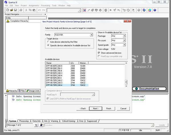
next page, the wizard will prompt you to add new files. Since there are none, just press next. On the next screen, you will select the family and device settings for the FPGA. First select the appropriate family. In our case, the FPGA we are using is a EPF10K7ORC240-4, and is part of the FLEX10K family. So go ahead and select it, as so:
We do not need any other EDA tool, so go ahead and click Next on the following page. Finally it will show you a summary of your new project. Click on Finish. You now have a project!
3. First go to File -> New. You will see a menu with several options. Select "Block Diagram/Schematic File" and press OK. You now have a schematic file called Block1.bdf open in front of you. This is where you will design your circuit.

4. In this tutorial, we will build a basic logic circuit to turn on and off the digit 1 decimal point. We will use both push buttons to control the decimal point, specifically when both buttons are pressed, the decimal point will be off. If only one button or neither button is pressed, then the decimal point will be on. As mentioned previously, turning off a segment happens when you set that segment to high, and turning on a segment happens when you set that segment to low.
5. Now that we know what we want our circuit to do, let's design it. We have two inputs (the two buttons) and we will lay that first. Click on the AND gate symbol on the left of the block schematic and you should see the Symbol Menu. Under Libraries, open up Primitiaves and then the Pin subfolder. You should see three types of symbols, bidir, input, and output. What we want is input for now, so click on input and press okay.

6. Now place the input pin on the left of the schematic. Since we have two inputs, do this twice. Now we should have two input pins on the left of the schematic. We now need to rename these input pins however. Double click on the pins and rename them to button1_input and button2_input.
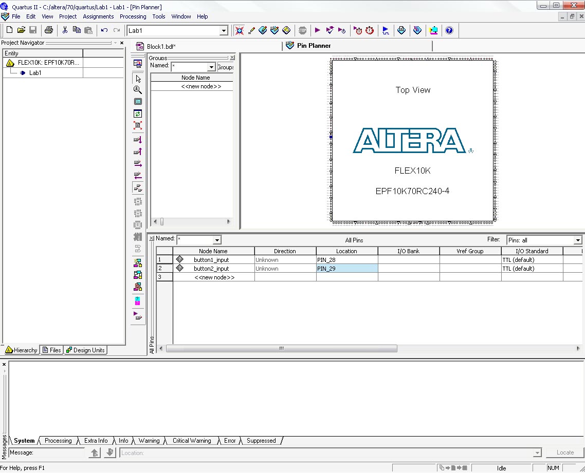
7. We now assign them to the proper ports on the FPGA (right now, these are just empty input pins, connected to nothing. We need to tell the FPGA which pins these actually are). We now assign the pins to the proper port on the FPGA. Right click on the input pin and go down to Locate, and then click on Locate in Pin Planner. You should see the pin planner screen, which lets yhou assign the location to each of your pins. In the button1_input row, double click on the Location column. You should see all the pin numbers for your FPGA. Refer to page 11 to see the Push Button numbers.
Since button 1 is pin 28, and button 2 is pin 29, change the value in the location column to reflect those pins numbers. (Hint: if you type 28 in the box, it will automatically find Pin_28). Do this for both inputs.
8. Now let's bring out the output pins. We only have one output pin for this basic circuit, the Digit 1 decimal point, so place an output pin on the schematic. Rename it to digit1_decimal. Right click on it again to go to "Locate in Pin Planner" and set the location for digit1_decimal. Refer to your instruction booklet to see the actual pin numbers for those segments on page 12. We see that Digit 1 Decimal is pin 14, so set digit1_decimal to that.
9. Now we have our inputs and outputs placed on the schematic. We now need to add the logic gates to make our circuit work. We want the decimal point to light up when either both buttons are pressed, are neither button is pressed. If one and only one button is pressed however, the decimal point should not be lit. Let's draw out the truth table for this to see what we need done.
X Y | Output
0 0 | 0
0 1 | 1
1 0 | 1
1 1 | 0
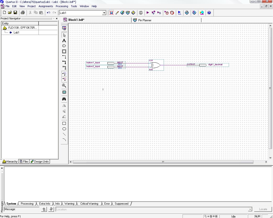
From the truth table, it becomes clear that the output is simply equal to input 1 XOR input 2.
10. Go back into the symbol menu, and go under primiatives and then under logic. You will see many basic types of gates, such as AND, OR, and NOT gates. Go down until you find the XOR gate and place that on the schematic. Connect the two inputs into XOR gates by dragging the wire towards it. Likewise, connect the output to the XOR gate. Your basic circuit now is complete.
11. Now let's save our schematic. Go to File and Save it into your project directory Lab1. Save it as Lab1.bdf.
12. Now we can start testing our schematic on our hardware board. Go to the Processing Menu and go to Start Compilation. It will start compiling your schematic and at the end should give you a sucessful screen. Note, if you have errors, read the error messages to see what the problem was.

13. Now we can program our hardware board. Make sure your jumper settings are correct and that the AC Adapter is connected! Go to Tools and then Programmer. First click on Hardware Setup and click on Add Hardware. Set Hardware Type to ByteBlaster II and Port to LTP1. Click on Okay. Then in Currently selected hardware, choose ByteBlasterII (LPT1). Close the menu. Then check the Program/Configure checkbox. Now press Start.
14. If you were successful, your board should be running. Because by default all the segments are low, they will all be lit red. Now let's test your decimal point. Press one button. The decimal point should be go off. Press both though and the decimal point should be red again.
15. Congratulations! You have just finished your first circuit! But as mentioned above, the segments are lit red by default since an output of low turns on each segment. Let's update our circuit so that all the segments except our decimal point is off. There are 16 output segments in all, and we already have 1 (digit 1 decimal point), so we need to add 15 more output pins. Go ahead and place 15 more output pins on your schematic and rename them digit1_A, digit1_B, etc. Set the pin assignment of each pin like before. The pin numbers for the segments are on page 12 of your instruction manual.

16. To turn off the segments, we want to send a value of "high" to these outputs. Therefore, find the VCC symbol (it is under Primitves/Other) and place it on your schematic. Connect this to each of the output pins.

17. Compile and program your FGPA board again with your new circuit. Ignore the "Output stuck at VCC" warnings. Don't forget to save the updated schematic! The Segment Display will now all be off except your decimal point.
18. Congratuations! You now know the basic steps in creating a schematic and running it on your FPGA board. However, what makes EDA tools so powerful is that you can simulate them on your computer without ever having to run them on a hardware board. Also, by simulating your circuit, you can see important timing values for your logic. You will also run some timing simulations to see the timing diagrams for your circuit.
19. Generally speaking, there are two types of simulations - functional and timing. Functional simulations pretend that the circuit has no delays, and thus everything happens simulatenously (i.e. when an input changes, the output changes at the same exact time). Timing simulations however take into consideration the delays that are inherent in a circuit.
20. Let's first do a functional simulation. Go to File -> New and click on the Other Files tab. Click on the last option, which is Vector Waveform File. You should see an empty waveform display. Double click the left panel (the one with Name, Value) and you should see a pop up menu. Click on Node Finder and in Filter, choose Pins: input. Click "List." Select both input pins and add to the right window. Click OK. Now you will see those inputs on the left panel. Double click on the left panel again and for Type, choose OUTPUT. Then go to Node Finder again and for Filter, choose Pins: Output. Click on List again and you should see a list of all the output pins. Click on digit1_decimal and click on OK (note we do not care about the other outputs).
21. You should now see 3 pins on the left panel. On the left panel, select button1_input and right click and go to Value -> Count Value. You will see a pop up menu, click on the Timing tab. Make sure your start time is 0, your End Time is 1.0 uS, Count every is 10 ns, and your Multiplied Value is 1. Do the same for the second input, but change the Multiplied Value to 2. Save your waveform file as Lab1.vwf. Next go to Assignment -> Menu Settings, and choose Simulator Settings. In the Simulation Mode drop down menu, change it to Functional. In the Simulation input, select the vwf file you just saved. Click OK.
Brief explanation: Count Value means the signal will be periodically switched between 0 and 1. "Count every" is the switching period; and if the "Multiplied by" value is 2, the period will be doubled. We give different periods for different input signals so that we can see the output behavior with various input signals. Essentially, we will get every possible combination of inputs on our timing and functional diagrams, and thus can see the output for every combination of input.
22. Next, go to Processing -> Generate Functional Simulation Netlist. Then once it is sucessful, go to Processing -> Start Simulation. You can see the simulation results (zoom in and out to get a better view of the waveforms by right clicking on the timing axis). You can see how changing the input values changes the output values. When one input is high and one input is low (corresponding to you pushing just one button), notice how the output to the decimal point is high (which turns it off). Likewise, when both inputs are high or both inputs are low (corresponding to you pushing both buttons or neither button), the output is low (which turns on the decimal point).

23. Now let's try this with timing. Go back into Simulator Settings and change Simulation Mode from Functional to Timing. Change the Count Value for your two inputs so that the "Count every" is 100 ms now instead of 10ms. Then go to Start Simulation again. You will see a similar waveform, except this time you will see the delay in the output.

24. Congratuations! Now you have learned how to do basic functional and timing simulations with your circuit. Make sure you understand the overall design process with Quartus II. Future labs will depend on your ability to come up with a logical circuit and run it properly.