
In this tutorial, we will see a top-down design flow for the computer system described
in Lab4. We start from the understanding of the overall architecture, and then move to
the details of each building block.
Before we go to the architecture of a computer, let's discuss how people perform
calculations. First people need an algorithm to be run, and some paper as well as
a calculator. Then people read the first instruction in the algorithm, perform the
corresponding operation in the calculator, and write down the intermediate results on
papers. After the current instruction is finished, the next instruction will be executed,
until no more instruction left. The following figure shows this flow.
Basically people organize the computation by reading instructions from a program
and operating on the tools.
The computer system in Lab4 has a very similar flow. Memory block and program
counter are used to hold program and output the current instruction. Datapath module
and registers perform each instruction and store the intermediate results. Control logic
is the bridge between them. It compiles each instruction to the control signals needed
by the datapath module and registers. The next figure shows the architecture.
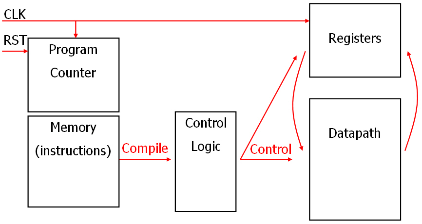
At the beginning of each clock cycle, program counter will give the address of
the current instruction. Then the instruction will be read into the control logic
block and compiled to the corresponding control signals. According to the control
signals, datapath module will perform proper activities and get result ready to
the input of registers. When the next clock cycle arrives, the result is written to
the registers, and the new instruction starts to run.
Based on the previous description, here are the function descriptions of these
building blocks.
The building blocks are implemented one by one, and then assembled together.
Control logic should be designed after other blocks. Therefore we know what are
the control signals needed and how to operate on them. In the following sections
we will discuss the details of each building block.
Memory is used to store program. Therefore the word length of the momoery
block should be equal to the length of each instruction. In Lab4, each instruction
consists of 8 bits. The depth of the memory in this lab is set to 16. Hence we
need a memory block can hold 16 8-bit words. Xilinux provides 16 by 1-bit ROM
block ROM16x1. It can be used to store 1-bit information in the total 8 bits. Then
we need 8 ROM16x1 blocks to construct memory block. They share the address
inputs, and each of them outputs one bit of the data.

Now we have the memory block to hold program. The next step is to put our
program into the memory block. Because it is read-only memory, we should define
the content as initial values of the ROM16x1s. The following part will show how
to translate a program to initial values.
Here is a simple program to perform 01001+00011.
1. Init
2. Move1 01001
3. Move2 00011
4. Add
According to the coding rule in lab4 description, the previous program can be
compiled to the following binary code in memory.
| Address | D(7) | D(6) | D(5) | D(4) | D(3) | D(2) | D(1) | D(0) | Instruction |
| 0000 | 0 | 0 | 0 | 0 | 0 | 0 | 0 | 0 |
Init |
| 0001 | 0 | 0 | 1 | 0 | 1 | 0 | 0 | 1 |
Move1 01001 |
| 0010 | 0 | 1 | 0 | 0 | 0 | 0 | 1 | 1 |
Move2 00011 |
| 0011 | 1 | 0 | 0 | 0 | 0 | 0 | 0 | 0 |
Add |
| 0100-1111 | 0 | 0 | 0 | 0 | 0 | 0 | 0 | 0 |
Init |
Finally the initial values are obtained by looking at the binary numbers on every
bit positions. (Refer to the slides of 5/18 discussion session)
| 11 11 |
11 10 |
11 01 |
11 00 |
10 11 |
10 10 |
10 01 |
10 00 |
01 11 |
01 10 |
01 01 |
01 00 |
00 11 |
00 10 |
00 01 |
00 00 |
Initial Value |
|
| D(7) | 0 | 0 | 0 | 0 | 0 | 0 | 0 | 0 | 0 | 0 | 0 | 0 | 1 | 0 | 0 | 0 | 0008 |
| D(6) | 0 | 0 | 0 | 0 | 0 | 0 | 0 | 0 | 0 | 0 | 0 | 0 | 0 | 1 | 0 | 0 | 0004 |
| D(5) | 0 | 0 | 0 | 0 | 0 | 0 | 0 | 0 | 0 | 0 | 0 | 0 | 0 | 0 | 1 | 0 | 0002 |
| D(4) | 0 | 0 | 0 | 0 | 0 | 0 | 0 | 0 | 0 | 0 | 0 | 0 | 0 | 0 | 0 | 0 | 0000 |
| D(3) | 0 | 0 | 0 | 0 | 0 | 0 | 0 | 0 | 0 | 0 | 0 | 0 | 0 | 0 | 1 | 0 | 0002 |
| D(2) | 0 | 0 | 0 | 0 | 0 | 0 | 0 | 0 | 0 | 0 | 0 | 0 | 0 | 0 | 0 | 0 | 0000 |
| D(1) | 0 | 0 | 0 | 0 | 0 | 0 | 0 | 0 | 0 | 0 | 0 | 0 | 0 | 1 | 0 | 0 | 0004 |
| D(0) | 0 | 0 | 0 | 0 | 0 | 0 | 0 | 0 | 0 | 0 | 0 | 0 | 0 | 1 | 1 | 0 | 0006 |
In the simple instruction set, there is no branch or jump commmand. Hence we
only need a regular 4-bit counter as the program counter, to explore the 16 words
in the memory one by one. Xilinux provides a 4-bit counter CB4CE. It has clock
and clock enable inputs as well as an asynchronous clear input. The output is a
4-bit bus, which should be connected to the address port of memory block.

Imagine that the 4-bit counter starts from 0000 and increases one in every
clock cycles. The program will be read from the memory data port one
instruction by one instruction.
There are three 5-bit registers R1, R2, R3 and two 1-bit flags OV_FLG,
GE_FLG in the system to store data. Each bit needs a flip-flop. Besides
the flip-flops, let's look at the operations on the registers block. Every
instruction will affect the values of registers. Initialize command clears
all the registers; move1, move2 and store commands change the value
of R1 or R2; other arithmetic operations change the value of R3 or flags.
Therefore we need the capability to clear the registers and indicate which
register should load data from where.
By using D flip-flop FDRE, we can clear each bit and enable each bit to
read data. The last problem is the data source. From the instruction set,
we know that R1 only read data from memory, R3 and flags always read
data from datapath module, R2 may read data from memory or R3.
Hence the registers block needs two 5-bit data ports, one from memory,
the other from datapath. The following figure shows the structure of register
block. 
Let's consider one input combination as an example. If R1_en=1 and all other
control signals are 0s, R1 will read in the data from memory, which is a Move1
command.
According to the instruction set, there are four arithmetic operations, add, shift,
compare and mask. We need four 5-bit blocks to perform these operations.
Xilinx provides 8-bit adder ADD8, 8-bit comparator COMPM8 and 8-bit shifter
BRLSHFT8. They can be modified to perform 5-bit operations. Mask operation
is quite simple. There is nothing more than 5 AND gates in parallel.
Every operations use R1 and/or R2 as operands, and they share the input ports.
Besides the flag outputs, data outputs are shared by add, shift and mask operation.
A mux is added to select one operation result to the data output port. In addition,
2-bit shift offside control signals are needed for shift operation. The following figure
shows the structure of datapath module.

If sel(1:0)="01", the datapath module will perform R1+R2. The result will be
available at dpath_D(4:0) and the flag bit OV.
So far, we already built memory, program counter, registers and datapath
module. The last step is to design control logic, which is a bridge between
instructions and control signals. The inputs of control logic are the instruction
bits from memory, the outputs are the control signals needed by registers
and datapath module. Essentially, control logic is a truth table describes the
function of each control signal.
Consider the instruction Init which has instruction code "000". All the registers
are cleared by this command. Correspondingly, the clr input of registers block
should be 1 and all other control signals are 0s. Another example is Add,
which has instruction code "100". R3 and the overflow flag will be set by the
results from ADD5 block. Then R3_en and ov_en should be 1s, sel(1:0) should
be "01", and all other control signals are 0s. The following table gives a sample
of control logic.
| Instruction | D(7) | D(6) | D(5) | D(4) | D(3) | clr | R1_en | R2_en | R2_sel | R3_en | ov_en | ge_en | sel(1:0) | shf_of(1:0) |
| Init |
0 |
0 |
0 |
s1 |
s0 |
1 |
0 |
0 |
0 |
0 |
0 |
0 |
00 |
00 |
| Move1 |
0 |
0 |
1 |
s1 |
s0 |
0 |
1 |
0 |
0 |
0 |
0 |
0 |
00 |
00 |
| Move2 |
0 |
1 |
0 |
s1 |
s0 |
0 |
0 |
1 |
0 |
0 |
0 |
0 |
00 |
00 |
| Store |
0 |
1 |
1 |
s1 |
s0 |
0 |
0 |
1 |
1 |
0 |
0 |
0 |
00 |
00 |
| Add |
1 |
0 |
0 |
s1 |
s0 |
0 |
0 |
0 |
0 |
1 |
1 |
0 |
01 |
00 |
| Shift |
1 |
0 |
1 |
s1 |
s0 |
0 |
0 |
0 |
0 |
1 |
0 |
0 |
00 |
s1s0 |
| Comp |
1 |
1 |
0 |
s1 |
s0 |
0 |
0 |
0 |
0 |
0 |
0 |
1 |
11 |
00 |
| Mask |
1 |
1 |
1 |
s1 |
s0 |
0 |
0 |
0 |
0 |
1 |
0 |
0 |
10 |
00 |
For the VHDL implemention of a truth table, please refer to the slides of 5/18
discussion session.
After we implement all the building blocks, we finally put them together in the
top-level diagram. Program counter outputs to memory block; memory block
outputs data to registers and instructions to control logic; datapath read data
from registers and write back the results. The top-level diagram should be
similar to the following diagram.

To verify the correctness of the system, we put a test program to the memory
block. Here is a simple test program.
0 init
1 mov1 10101
2 mov2 00110
3 add
4 stor
5 mov1 00001
6 add
7 stor
8 shift 10
9 stor
10 mov1 00111
11 comp
12 mask
13 Init
14 Init
15 Init
The correct simulation result is shown in the following graph.
