What's flip-flop?
Flip-flop is a kind of component which can hold the output unchanging with the data input but read the data at the clock edge. The first example is D flip-flop FDCE:
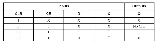
From the function table we know that when clock is enabled and jump from '0' to '1' D will be set to Q, otherwise Q keeps unchanged. CLR is used to set initial value '0' to the output Q. If the initial value is set to '1', it's FDPE:
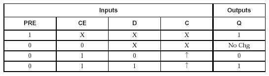
D flip-flop means the flip-flop reads data from a data input. There are also other flip-flops. Here is a toggle filp-flop FTCE: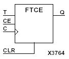

The difference between D flip-flop and toggle flip-flop is that the new output value for toggle flip-flop is the inverse of previous value, not the value of data input.
For more information please refer the libraries guide: Lib.pdf
Back to Top
What should be included in the report for each design?
In general there are four steps to finish one design: 1) design the circuit by drawing a schmetic diagram 2) verify the correctness by behavior simulation 3) find out the critical path by checking the timing report 4) demonstrate the critical path by post-place&route simulation. Therefore we need these four parts in the report.
Schematic Diagram:
Behavior simulation: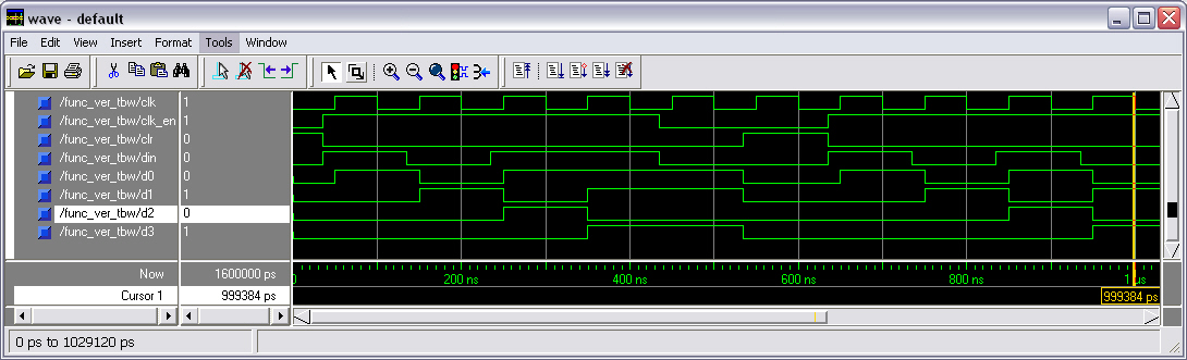
Timing report:
Post-place&route simulation timing diagram:
Back to Top
What's the exact function of each design?
Refer to the slides for the discussion hour on 4/27.
How to design the circuits?
Refer to the slides for the discussion hour on 4/27.
When a counter failed?
From the post-place&route simulation we know that output signals are not valid as soon as clock jump from '0' to '1'. The worst delay could be small or large. To guarantee we don't mistake any unstable signal or miss any valid signal, a design rule of sequetnial logic is that all signals triggered by a positive clock edge must be valid before the next positive edge and until the next positive edge. Based on this concept, an asynchroneous counter failed means an ouput signal is not valid before the next positive clock edge.