Name1:___________________________ Name2:___________________________
Lab Assignment #5, Due December 5, 1997
Due 5:00PM, to
be placed under the door of AP&M'4840
Introduction: This lab consists of two parts. In the first part
you will build a controller for the "Two's Complement Multiplier", whose
datapath was implemented in the second lab, on LogicWorks. In the second
part of the experiment, you will implement a traffic light controller on
a breadboard.
Part 1: Two's Complement Multiplication
The datapath for the 8-bit Two's Complement Multiplication is given in
the following figure. For this lab, you can either use your own datapath
designed during the second lab, or use the multiplier provided here
in this page.

The algorithm for two's complement multiplication was given as the following:
-
Load multiplier and multiplicand, clear accumulator A, reset flip flop
F
Repeat
-
if the rightmost bit of the multiplier is 1 then A = A + Multiplicand
-
Shift A and Multiplier to the right
Until count = 7
-
Correction step
If the rightmost bit of the multiplier is 1 (multiplier is negative)
then A = A - Multiplicand
-
The result can be found in A(7:0)Multiplier(7:1)
The control signals have been defined as in the following table, originally
provided in Lab#2. In this experiment, you will build a controller
to implement this. However, this time we will modify the algorithm somewhat
to ease the implementation and speed up the multiplication. The amount
of speedup will depend on the multiplier input to the circuit.
| Cycle |
End |
LoadI |
ClearA |
LoadA |
Shift |
Add/Sub |
ResetF |
| 0 |
0 |
1 |
1 |
0 |
0 |
0 |
1 |
| 1,3,5,7,9,11,13 |
0 |
0 |
0 |
1/0 |
0 |
0 |
0 |
| 2,4,6,8,10,12,14 |
0 |
0 |
0 |
0 |
1 |
0 |
0 |
| 15 |
0 |
0 |
0 |
1/0 |
0 |
1/0 |
0 |
| 16 |
1 |
0 |
0 |
0 |
0 |
0 |
0 |
The modifications are:
-
Combine the control signals LoadI, ClearA, ResetF (since they have the
same logic level for all clock cycles) and call the new signal Reset.
-
Convert the clock cycles 1-14 into a loop of length 7, where each step
of the loop consists of either one or two cycles depending on the value
of the least significant bit of the multiplier at a particular instant.
When we incorporate the following modifications in the design we end up
with the following state diagram. (Others in this state diagram refer to
all remaining not explicitly specified signals.)

The state diagram has five states. The first state is the state where
the multiplier waits for the begin signal. In this state, the data at the
inputs of the multiplier and multiplicand registers will be loaded to the
registers continuously, the accumulator will be cleared and the flip-flop
will be reset. When the Begin signal is asserted the multiplier will start
to multiply by advancing to the state S1 or S2 depending on the least significant
bit of the multiplier. In state S1 the multiplicand will be added to the
accumulator, which contains the most significant byte of the partial sum.
In state S2, the accumulator and the multiplier will be shifted to the
right and the counter will be incremented (counter will be incremented
during the falling-edge of the clock signal). State S2 can be followed
by four states depending on the value of the least significant bit of the
multiplier at that instant and the value of the counter. If counter <
7 (the condition counter < 7 is equivalent to that of counter != 7,
in this context) the next state will be either S1 or S2 depending on the
value of the Mul, otherwise the next state will be S3 or S4 depending on
value of the Mul. There are some state transitions which are not shown
in this current state diagram. Independent of the current state, when you
assert a low Begin signal at any time, the next state must be S0. In order
to be able to simplify the design procedure, you can derive your next state
equations without considering the Begin signal and then connecting the
Begin signal to the reset inputs of the flip-flops. This way you will need
to worry about one less signal when you derive your state equations.
You are supposed to design the controller as a state based design. The
overall structure of your controller design should look like the one in
the following figure.
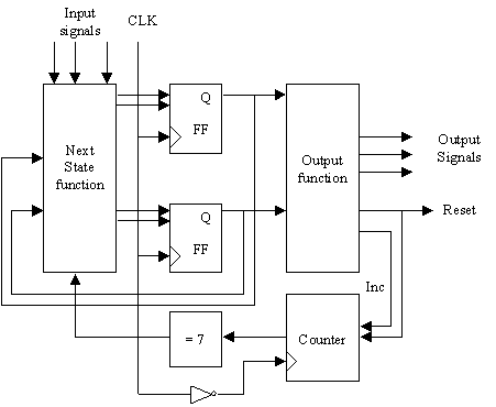
The flip-flops shown in this figure must be positive-edge triggered.
Test your flip-flops before starting your design and if they are not positive-edge
triggered invert, the clock before connecting the CLK inputs of the flip-flops.
In order to be able to implement the controller, you need to follow
the steps given below.
-
Find out the number of flip-flops necessary. Use JK flip-flops for this
design. For state encoding, use natural binary encoding scheme (i.e. S0
= '0000', S1 = '0001', ...)
-
Derive the truth tables for the output signals and for the JK inputs of
the flip-flops
-
Using simplification techniques, implement the output and input functions
using the truth tables.
After implementing the controller, connect the controller to the datapath
given (or your own), and report the intermediate register values and control
signal values for every clock cycle for the multiplication of the following
pair of numbers (all numbers are in Hex).
-
Multiplier = F2, Multiplicand = 87
-
Multiplier = F0, Multiplicand = 20
-
Multiplier = 20, Multiplicand = F0
-
Multiplier = 60, Multiplicand = 25
Part 2: Traffic Light Controller
In this part, you will implement the following traffic-light controller
on breadboard:
Four traffic lights will point in four directions, identified by the
letters N, S, W, and E. Each light will go through the following sequence:
green (15 seconds), yellow (5 seconds), and red (20 seconds). Furthermore,
the N and S lights will always be the same color, as will the E and W lights,
and the N-S lights will never be green or yellow at the same time as the
E-W lights.
In this implementation, you are given a reference clock which generates
a pulse every second. Using this reference generator as the input to your
circuit, implement the traffic light controller on a breadboard. The control
structure will look like the one in the first part of this experiment.
The state flow should be as follows
-
Reset Counter, N-S is green
-
Wait for 15 seconds
-
Reset Counter, N-S is yellow
-
Wait for 5 seconds
-
Reset Counter, E-W is green
-
Wait for 15 seconds
-
Reset Counter, E-W is yellow
-
Wait for 5 seconds
Using the above given state flow, generate the state diagram and then implement
the circuit corresponding to this state diagram on a breadboard. The overall
structure of the traffic light controller should be as in the following
figure:

TA Signature ________________________________________
If you do not want to spend too much time while building your circuit
on breadboard, design your circuit on LogicWorks before implementing. Also
while designing the circuit consider the components available in your lab
kit.
Requirements:
For both parts of this experiment, please return your truth tables,
next state functions, and output functions. For the LogicWorks part, return
a printout of your implementation of the control logic together with the
required results of the simulations. Please use the same format as in the
example
while providing your simulation results.