Name1:___________________________ Name2:___________________________
Lab Assignment #3, Due November 07, 1997
Due 5:00PM, to
be placed under the door of AP&M'4840
Introduction: This lab consist of two parts: (i) Implementation
of an error correction circuit for a specific code on LogicWorks, (ii)
Measurement of delay of an inverter gate, and delay of a multi-level implementation
of a logic function with implication and inhibition gates.
Part 1: Error Code Correction
It is reputed that the ancient Phrygian civilization (Distant neighbors
of the Elamites of your first midterm fame!) used a base-6 number system
and that they furthermore had developed a computer that represented base-6
numbers! In order to represent a base-6 number they had developed a (rather
inefficient; it used 8 bits instead of the minimum 3!) code as follows:
| 0 |
10010001 |
| 1 |
10001010 |
| 2 |
01010010 |
| 3 |
01001100 |
| 4 |
00110100 |
| 5 |
01100001 |
In order to understand this exercise, think about the following points.
How many 1s and 0s does each 8-bit code have? What is the sum of
the indices of the bits that have 1s? Consequently, starting
from a legal word, how many bits need to be simultaneously flipped in order
to produce another legal word?
You are asked to develop an error-correcting code, by understanding
the Hamming distance of the aforementioned code and generating the appropriate
logic circuitry for correcting all errors that can be corrected according
to the Hamming code distance analysis. In order to do this, you will need
probably to sum the indices corresponding to the non-zero entries and subtract
this sum from the invariant sum of the word entries in the illustrated
code words. In addition to the sum, you will need to identify the location
of the faulty bit. A convenient circuit that will let you identify the
faulty bit index is a decoder shown here.

As can be seen on the figure, the decoder has three inputs (S2..0).
Depending on the value of the inputs, one of the outputs of the decoder
becomes a 1, all of the others are zero. Since an XOR gate with one input
connected to 1 acts like an inverter gate, depending on the value of the
inputs to the decoder, the corrupted bit will be flipped (inverted), thus
the erroneous word with one bit error will be corrected.
In order to sum the indices of the non-zero entries, you can use the
multiplier circuit that you have constructed in your first lab. In that
circuit, the multiplier was placed in the Q register and a right-to-left
scan of the multiplier bits provided us the signal for adding the multiplicand
onto a repeatedly shifted partial sum. While a right-to-left scan is still
useful in this context, a shift of the accumulator is no longer needed
(remember this is no longer a positional number system) and instead of
adding the multiplicand, you need to add the index of the bit in the Q
register. You can achieve this by incrementing the M register (starting
from 1), which should correspond to the index position of the bit being
scanned in the M register.
The algorithm is given as follows:
-
Accumulator = 0, Counter = 1, Multiplier = Code
-
Repeat 8 times
-
If least significant bit of Multiplier is one Accumulator = Accumulator
+ Counter
-
Shift Multiplier to the right, Counter = Counter + 1
-
End
Even though the control logic given in the previous lab had a different
purpose, you can still use that control logic to implement this algorithm.
All you have to do is to modify the datapath of your circuit such that
it will implement the above algorithm. For this part, we will add a "counter"
to the CSE140L library. The counter will have
a low active load input, which will set the counter output to 1, and a
high active increment input which will increment the counter every clock
cycle. Mac Users CSE140L
You are asked to the following:
-
Identify the error correction needed and define a strategy for implementing
it in line with the above comments
-
Modify the datapath according to the given hints.
-
Simulate your circuit with the following data:
-
10110001
-
11010010
-
00110101
-
00100001
-
00101100
Part 2: Logic Functions
The object of this part of the exercise is twofold. You are asked to develop
experience with measuring delays through a logic circuit and also to get
some understanding for the possible implementation of a circuit . We will
use the circuit that you develop for the latter as a measurement tool for
the former objective also.
As you have seen in your text, Gajski, Principles of Digital Design,
Ch-3, multiple variant implementation of the same circuit exist. Besides,
canonical, standard, and nonstandard forms, another dimension in constructing
such circuits, is the type of complex gate discussed in section 3.9, such
as AOI and OAI gates. Such complex gates frequently do not share axiomatic
bases that define the operators of Boolean algebra. Neither is it straightforward
to develop methods and approaches for the simplification of such complex
gates.
While the inhibition ('@') and the implication ('#') operators (defined
in Section 3.7) are in same sense primitive logic operators of two variables,
they also share a number of characteristics of the aforementioned complex
gates. We ask you to map a function given as a sum-of-minterms to a form
that can be expressed as a combination of inhibition and implication gates
(no other gates, not even inverters, even expressed as inhibition or implication
gates can be used). After implementing the given function in this form
you are asked to measure its delay.
In actual implementation of logic gates, there is a delay between the
time at which the input is changed and the time at which the effect of
the input change is observed at the output. Our aim is to measure the propagation
delay of an inverter gate. The propagation delay of a gate is defined as
the average time needed for input change to propagate to the output. The
output of a gate can go from L to H, or H to L. The propagation delay for
L to H is defined as tplh and the propagation delay H to L is
defined as tphl . The average propagation delay can be defined
as the average value of tplh and tphl . Therefore,
Further information about propagation delays can be found in Gajski,
Principles of Digital Design, Ch-3. Since the delay of an inverter
gate is usually less then 10ns, we cannot directly measure the delay of
an inverter gate. Therefore, we will build a circuit called a ring oscillator
(odd number of inverters connected like a ring) and measure the period
of oscillation in order to determine the average propagation delay of an
inverter gate.
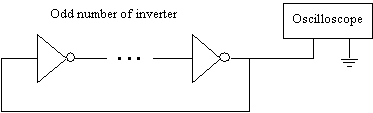 The figure shows a ring oscillator. In order for the ring oscillator
to oscillate you must have an odd number of inverters connected in a ring
fashion. You can choose the output of any inverter to observe the waveform
and measure the period of oscillations. Use at least three inverters.
If you choose to use three inverters, the period of oscillations will be
6 times the propagation delay of an individual inverter gate. When you
measure the propagation delay of an inverter gate, get the TA's signature
and let them verify your measurement. You will need to use this setup to
measure the delay of the logic function implementation.
The figure shows a ring oscillator. In order for the ring oscillator
to oscillate you must have an odd number of inverters connected in a ring
fashion. You can choose the output of any inverter to observe the waveform
and measure the period of oscillations. Use at least three inverters.
If you choose to use three inverters, the period of oscillations will be
6 times the propagation delay of an individual inverter gate. When you
measure the propagation delay of an inverter gate, get the TA's signature
and let them verify your measurement. You will need to use this setup to
measure the delay of the logic function implementation.
tplh =
tphl =
tp =
Signature: _________________________________
How to measure delay of a logic function:
-
Find an input combination such that inversion of one of the inputs will
invert the output.
-
Apply a square wave to that input. The period of the square wave should
be larger than twice the propagation delay of the boolean function for
that particular input.
-
Observe both input and output wave form on the oscilloscope simultaneously
in order to measure the propagation delay
As an example: Suppose the logic function is F = ABC. For the input combination
B = 1, C = 1, inversion of the input A will invert the output. Therefore,
connect a square wave to the input A, and observe both waveforms simultaneously.
The waveforms should look like the waveform given in the following figure.

Then measure the propagation delay of the circuit for the particular
input you choose. Measure both L to H and H to L delays and find the average
propagation delay.
You will use your ring oscillator as a square wave generator for the
measurement of propagation delay. However, in order to get the period of
oscillations long enough you need to modify the ring oscillator circuitry
as in the following figure:
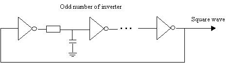
where the resistor is 330 ohms and the capacitor is 0.01 microF.
Implementation of a logic function with inhibition and implication
operators.
The inhibition operator is denoted by '@' and defined
as A@B = AB'
The implication operator is denoted by '#'
and defined as A#B = A + B'
The function you are asked to implement is:
The implementation should have the following form:
F = [? @ { (? @ ?) # (? # ?) }] # [? # { (? @
?) # (? # ?) }]
Where '?' represents any of the literals x,y, and z, but not their
complements.
You may find the following identities of inhibition/implication gates
useful in developing the desired function
-
x + y = y # ( y # x ) = x # ( x # y)
-
x + y' = x # y
-
y + x' = y # x
-
x' + y' = (x @ y) # y = (y @ x) # x
.
-
xy = y @ (y @ x) = x @ (x @ y)
-
xy' = x @ y
-
yx' = y @ x
-
x'y' = (y # x) @ y = (x # y) @ x
.
-
[y @ (y @ x)]' = [(y # x) @ y]
-
[x # y]' = y @ x
-
x # y = y' # ( y' # x)
-
x @ y = y' @ (y' @ x)
Implementation of implication and inhibition gates:

You are asked to do the following
-
Develop implication and inhibition gates out of your Lab Kit components,
as just shown.
-
Use the inhibition and implication gates only, to implement the given sum-of-minterms
form
-
For full credit implement this in the given form
F = [? @ { (? @ ?) # (? # ?) }] # [? # { (? @ ?) # (? #
?) }]
(If you can do this, you can skip part 2.)
-
Implement the circuit on a breadboard
-
Measure the propagation delays
Implement the circuit and fill in the following truth table. Use the switches
on the breadboard as the inputs so that they can be changed easily. Choose
one of the input combinations satisfying the condition given in "How to
measure delay of a logic function" and measure the propagation delays.
|
x
|
0
|
0
|
0
|
0
|
1
|
1
|
1
|
1
|
|
y
|
0
|
0
|
1
|
1
|
0
|
0
|
1
|
1
|
|
z
|
0
|
1
|
0
|
1
|
0
|
1
|
0
|
1
|
|
F
|
|
|
|
|
|
|
|
|
tplh =
tphl =
tp =
Signature: _________________________________
You are also required to check whether the operators of inhibition and
implication are 'commutative' and 'associative'. Starting from the previously
constructed implementation, implement the following functions and fill
in the truth tables.
-
Apply all possible commutativity at the primary inputs
-
Convert the implementation into this form:
F = [? @ { ( (? @ ?) # ?) # ? }] # [? # { ( (? @ ?) #?
) # ? }]
|
x
|
0
|
0
|
0
|
0
|
1
|
1
|
1
|
1
|
|
y
|
0
|
0
|
1
|
1
|
0
|
0
|
1
|
1
|
|
z
|
0
|
1
|
0
|
1
|
0
|
1
|
0
|
1
|
|
F
|
|
|
|
|
|
|
|
|
|
|
x
|
0
|
0
|
0
|
0
|
1
|
1
|
1
|
1
|
|
y
|
0
|
0
|
1
|
1
|
0
|
0
|
1
|
1
|
|
z
|
0
|
1
|
0
|
1
|
0
|
1
|
0
|
1
|
|
F
|
|
|
|
|
|
|
|
|
|
Requirements:
In part 1, do Bullets (1-3) and turn in a printout of your design.
In part2, do Bullets (1-5). Get your TA's signature and turn-in a report
outlining the simplification you have implemented and your results regarding
commutativity and associativity of the underlying gates as in the last
outlined part.