Shengye Wang (and Prof. Taylor)

Shengye has helpfully provided infrastructure for getting your designs
running on an FPGA. He has a JTAG cable that connects a computer to the FPGA
board, and has written the code that interfaces the core's I/O interface to the JTAG
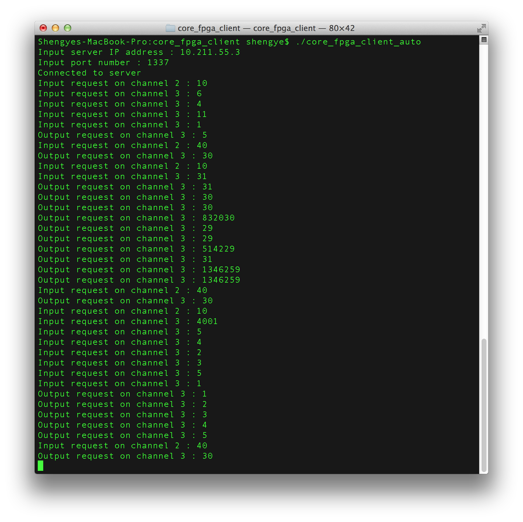
connection on the FPGA chip. After building with Quartus and downloading the FPGA .sof file, you can communicate
with your processor over the I/O channel using the PC's standard input and output. It looks like this:


Getting your design running on the FPGA:

To get your stuff running on the FPGA, you need to perform the following steps:
  1. Make sure your fib design works in timing simulation.

  2. Modify fib to output the result to an I/O channel

  3. Optionally modify fib to also get the input from an I/O channel.

  4. Be sure you are still using the "EP2C35F672C6" chip in your project.

  5. Create a new Quartus project with only your synthesizable files.

    (no extra files, please, no testbenches, and no io_devices.v).
    Add {core_fpga.v core_pll.v core_vjtag.v core_pll.qip core_vjtag.qip } in
    this directory to your project.


  6. Be sure that your core module has exactly the specified interface in Lab 3A (and works in timing simulation):
    // D_WIDTH : data width
    // PA_WIDTH : port (i.e. IO channel) address width
    
    module core#(parameter D_WIDTH = 34, PA_WIDTH = 4) 
                (
                input clk 
                , input reset_i 
                , input [D_WIDTH -1 : 0] in_data_i
                , input in_ack_i 
                , input out_ack_i
    	    , output in_req_o 
    	    , output out_req_o 
                , output [PA_WIDTH -1 : 0] in_addr_o
                , output [PA_WIDTH -1 : 0] out_addr_o
                ,  output [D_WIDTH -1 : 0] out_data_o
                );
    
    
  7. Open the pin planner in the assignments menu, and perform
    the following pin assignments.
    If the node name does not appear automatically, use "new node" to add.
  8. Select Device from Assignment menus to open the Device dialog.
    Click on Device and Pin Options, then Unused Pins, and then
    on the right choose "As input tri-stated with weak pull-up".
    This will make sure that unused pins on the FPGA that connect
    to the PC board do not "fight" with whatever they are wired to.

  9. Recompile the whole project, and then email the .sof file to
    Shengye (wang at shengye dot me) and also to the staff-141-taylor@googlegroups address with a brief instruction on what needs to be typed at
    the console, and what output to expect.