cse141L
Lab
2:
TrivialScalar Datapath
Changelog
| October 12 |
There are some minor changes in the datapath pdf and the wrapper provided. It's just signal name changes,
so that they abide to the naming conventions of the Coding Standards. Bring a hard copy of the report in class.
|
Due: October 14
Overview
In this lab, you will implement a datapath for a really simple processor that implements a very simple instruction set. It is
so simple, in fact, that it does not even have a branch instruction, so it cannot execute most programs. The processor does,
however, have all the parts that a real processor has: A fetch unit, decode logic, functional units, a register file, IO support,
and access to memory.
This lab is mostly about learning the skills you will need in the labs 4-6, and we structured it so that you can learn from each
other. All of you will be implementing the same datapath, so you will all run into similar problems. Learn from your classmates,
and then go apply what you learn to your own design.
Once you have mastered the skills here, you will go and apply them creatively to implementing your processor in labs 4 and 5.
NOTE: This lab can be performed in groups of two or three, but your groups must remain consistent throughout the duration of Labs 2 and 3.
On that same note, we encourage groups to help each other out (especially with tool problems).
Please remember that you must conform to the class
coding standards. They are
available here.
If you find a bug in them (e.g., they are causing you to do something horribly ugly), please let the professor
or the TA know.
The greatest common divisor example is
available here. Create a
new project and import all the files. If you
simulate using gcd_tbw.tbw, it will run a short test.
This example demonstrates the coding standards for
the datapath and the modules therein.
Getting Started
General Notes
- As in Lab 1, we will use "Virtex4 - XC4VLX15" as our target device.
-
This PDF details the datapath (for this lab) and the control signals (for Lab 3).
- This lab provides a tutorial for generating the memories that will be used in the TrivialScalar design.
- In order to be consistent with good coding practices in Verilog, we recommend that each student design in a modular fashion.
What we mean by this is that each module in the datapath diagram have all of the "logic" for that block within it and any
larger modules (e.g. the entire datapath) should consist of only instantiations and interconnections. If this isn't automatically
apparent, we would recommend reading through a couple of the tutorials listed at the bottom of this lab.
- All Verilog used in these labs should be synthesizable.
- All
reset signals should be asynchronous.
- IMPORTANT: It is recommended that you read through the entire lab then begin your implementation from the beginning.
Not doing so may make this lab more difficult than it needs to be.
Datapath Implementation
We'll start by implementing the top-level schematic for this lab: datapath.v.
Datapath
module datapath
(
	// All of these signals originate from the control section of the processor
	// Controls the operation of the processor, determining if it should be stalled, reset or running
	input [1:0] run_stall_reset_sel_in,
	// Tells the register file that we want to write this cycle
	input regfile_write_en_in,
	// Tells the dmem wrapper if we're going to read or write this cycle
	input dmem_read_write_req_in,
	// Selects from where the register file should derive its write input
	input [1:0] reg_sel_in,
	// Signals DRAM that it should write at the end of this cycle
	input dmem_write_en_in,
	// Tells the ALU which operation (ADD, SUB, MULT) it should perform this cycle
	input [1:0] alu_op_code_in,

	// This signal allows the control section of the processor access to the current instruction
	output [3:0] inst_out,

	// Global clock
	input clk,
	// Global reset
	input reset,

	// All of these signals come from or go to a module external to the processor
	// These signals are described in the IO section
	input [7:0] in_data, // From IO Device
	output [7:0] out_data // To IO Device
);
This is the top-level interface for your datapath. You should use this to connect to the control portion of your processor and to
the outer processor interface. You should just instantiate and connect all of the inner pieces that you'll be designing below in
this module.
Question 1: Using the definitions of the different modules below, go ahead and construct our top-level verilog file(datapath.v). Provide the source code.
Decode
// Parameters:
//	INST_WIDTH -> Width of an instruction
//	OP_CODE_WIDTH -> Width of the instruction's opcode field
//	LOG_NUM_REGS -> Log-base-2 of the number of registers (number of bits needed to identify a register)
//	IMM_WIDTH -> Width of an immediate
module decode#(parameter INST_WIDTH = 16, OP_CODE_WIDTH = 4, LOG_NUM_REGS = 2, IMM_WIDTH = 8)
(
	// Incoming instruction from the Imem
	input [INST_WIDTH - OP_CODE_WIDTH - 1 : 0] inst_in,

	// The encoded register bits (going to the register file)
	output [LOG_NUM_REGS - 1 : 0] r1_out,
	output [LOG_NUM_REGS - 1 : 0] r2_out,

	// The immediate (possibly ending up at the register file)
	output [IMM_WIDTH - 1 : 0] imm_out
);
The general ISA format is as follows: <4 bit opcode><2 bit R1><2 bit R2><8 bit Immediate>
With this in mind, there will be 9 different instructions and 4 different registers to choose from:
| Opcode |
Instruction Format |
Instruction Definition |
| 1 |
ADD R1 R2 |
R1 = R1 + R2 |
| 2 |
SUB R1 R2 |
R1 = R1 - R2 |
| 3 |
MULT R1 R2 |
R1 = R1 * R2 |
| 4 |
LD R1 R2 |
R1 = MEM[R2] |
| 5 |
ST R1 R2 |
MEM[R2] = R1 |
| 6 |
LI R1 <Immediate> |
R1 = <Immediate> |
| 7 |
READ R1 |
R1 = Input from IO |
| 8 |
WRITE R1 |
Output to IO = R1 |
| 9 |
HALT |
End of execution |
The decode module should just correctly parse the operands from each instruction and feed them into their specific modules.
Question 2: Design the decode.v file. Provide the source code.
ALU
// Parameters:
//	WIDTH -> Width of the incoming data (via the register file)
module alu#(parameter WIDTH = 8)
(
	// Incoming inputs from the register file
	input [WIDTH - 1 : 0] v1_in,
	input [WIDTH - 1 : 0] v2_in,

	// Opcode of the operation to perform (derived from the ISA)
	input [1 : 0] alu_op_code_in,

	// Result of the given operation
	output reg [WIDTH - 1 : 0] result_out
);
The ALU for this processor is fairly straightforward, as it only needs to implement three separate instructions: ADD, SUB, and MULT.
Using the opcodes and other ISA information listed in the Decode section, go ahead and design this module.
Question 3: Implement alu.v using the table in the Decode section and the information above. Provide the source code.
Instruction and Data Memories
There are two memory modules to be generated for this processor. One will be the instruction memory(imem), which will be a ROM, and the other
will be a data memory (dmem), which will be a RAM. You should use the provided verilog wrapper to access the dmem. For
those of you unfamiliar to wrappers, it will just act as a method for us to access the dmem. The wrapper is located
here. The wrapper is what you should be using throughout your code, and not the RAM module you are
about to generate. Also, please do not change the contents of the wrapper. If you find it not working properly, please notify the TA through email or the Blackboard.
Here's the interface for instantiating and communicating with a dmem module:
module dmem#(parameter A_WIDTH = 8, D_WIDTH = 8)
(
	// Global reset
	input  reset,
	// Global clock
	input  clk,

	// Used to specify either a read or a write
	// request.
	// 1 -> read/write request
	// 0 -> no requests
	input  dmem_read_write_req_in,
	// Assert for writing (write enable)
	input  dmem_write_en_in,
	// Address for data we'd like to retrieve
	input  [A_WIDTH - 1 : 0] addr,
	// Data input for writing
	input  [D_WIDTH - 1 : 0] din,
	// Data output for reading
	output [D_WIDTH - 1 : 0] dout,
	// Don't worry about this output
	output refused
);
Interfacing with the dmem should be fairly straightforward. All signals are edge-triggered.
Here's a basic overview of how each operation works:
-
Read --
read_write_req must be asserted (1) and the addr bus must be set to
the address we would like from the RAM. Your data should be available on the dout bus on the next edge.
-
Write --
read_write_req and write_en must be asserted and the addr bus must be set to the address
we would like to write to in the RAM.
Question 4: Go through the following tutorial to generate both the imem and dmem modules. In your report, please generate a diagram showing the interface you'll be using for the two modules (imem and dmem).
Memory Module Generation Tutorial
Generating Block (Synchronous) Memories [dmem only]
NOTE: The Xilinx Core Generator may not function correctly in Linux. Our experiences have yielded errors late in the generation process.
You can either brave it in Linux, or you can use the Windows version (in the lab, if need be). If you've had success with the Core
Generator in Linux, please let the TA know.
-
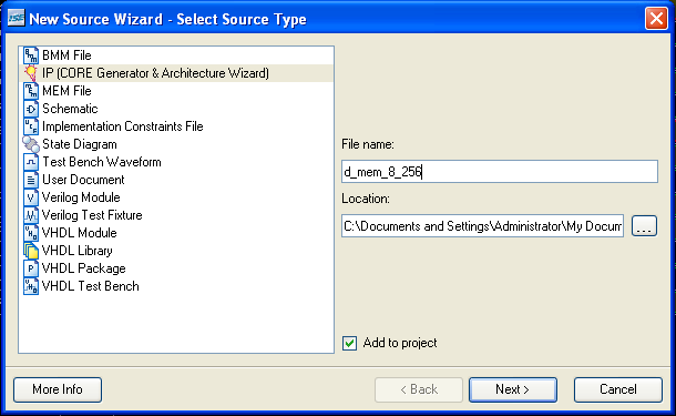
In the ISE viewer go to "Project"->"New Source". Select "IP (CORE Generator & Architecture Wizard)" on the left. Decide on a
file name for the particular component you're designing and type it into the "File name" field. The naming scheme in the screen-shot
below demonstrates a <memory type>_mem_<width>_<size> scheme. Please use the name written in the screen-shot below
for the
dmem module, as the wrapper depends on it being consistent. Click next at this point.
-
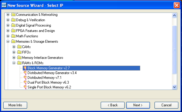
In the "Memories & Storage Elements"->"RAMs & ROMs" folder, choose "Block Memory Generator", click next, and then finish.
-
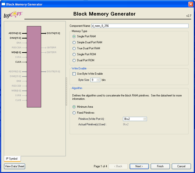
- Be sure that "Single Port RAM" is selected and then click next.
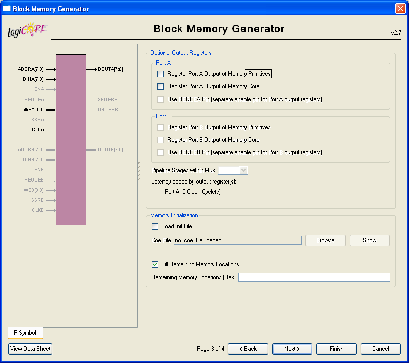
-
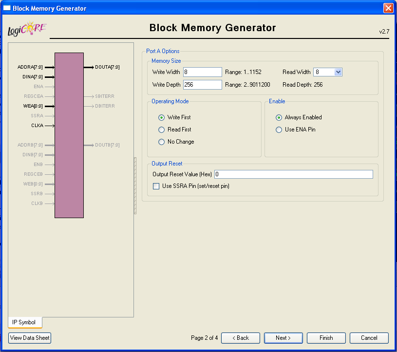
- Set "Write Width" to 8 and "Write Depth" to 256, meaning that you are generating a 8-bit wide, 256-entry memory module.
- Go ahead and click "next".
-
- Check the "Fill Remaining Memory Locations" box and confirm that the "Remaining Memory Locations" field is 0.
- Finally, click finish to generate the memory component.
-
Your memory module should now be imported into the project. For usage instructions, please consult the
*.veo file, which should now be located in your project directory.
Generating Distributed (Asynchronous) Memories [imem only]
NOTE: The Xilinx Core Generator may not function correctly in Linux. Our experiences have yielded errors late in the generation process.
You can either brave it in Linux, or you can use the Windows version (in the lab, if need be). If you've had success with the Core
Generator in Linux, please let the TA know.
-
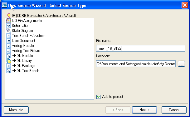
In the ISE viewer go to "Project"->"New Source". Select "IP (CORE Generator & Architecture Wizard)" on the left. Decide on a
file name for the particular component you're designing and type it into the "File name" field. The naming scheme in the screen-shot
below demonstrates a <memory type>_mem_<width>_<size> scheme. Click next at this point.
-
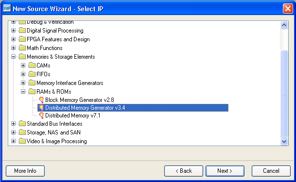
In the "Memories & Storage Elements"->"RAMs & ROMs" folder, choose "Distributed Memory Generator", click next, and the finish.
-
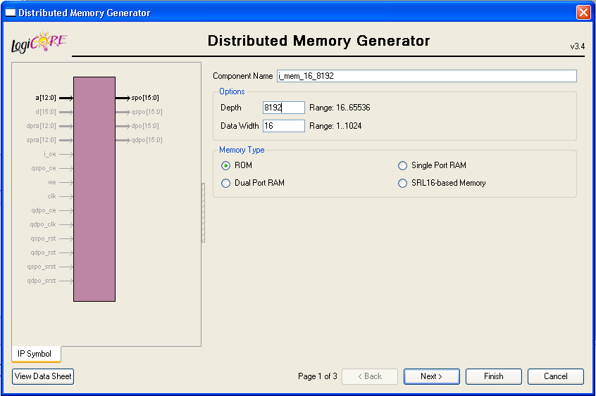
- Enter your desired depth into the "Depth" field (I would recommend something small--around 256, unless your really need a ROM of that size).
- Enter 16 as your "Data Width" (the width of an instruction).
- Select the "ROM" radio button and then click next.
-
Click browse and locate your desired coefficients (*.coe) file to preload the ROM with. For now you can use the
test program as a default file. More details on this will follow on lab 3.
Be sure that the "Default Data" box reads 0. Nothing else should be set here. Go ahead and click finish.
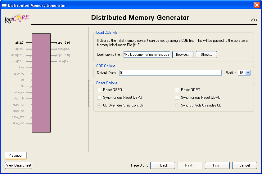
-
For usage instructions, please consult the *.veo file (one is generated for each module), which should
now be located in your project directory. Or, if you just want the module's inputs and outputs, highlight
the newly generated module and, in the processes tab, navigate to "CORE Generator"->"View HDL Functional Model".
Look for the "module" declaration directly under the "timescale" statement.
Register File
// Parameters:
// 	WIDTH -> Width of the data stored in each register
//	LOG_NUM_REGS -> Log-base-2 of the number of registers (number of bits needed to specify a register)
module reg_file#(parameter WIDTH = 8, LOG_NUM_REGS = 2)
(
	// Global clock
	input clk,
	// Global reset
	input reset,

	// Encoded register inputs
	input [LOG_NUM_REGS - 1 : 0] r1_in,
	input [LOG_NUM_REGS - 1 : 0] r2_in,

	// Data to be written on the next clock cycle
	input [WIDTH - 1 : 0] r_data_in,
	// Should we write this cycle?
	input regfile_write_en_in,

	// The asynchronous outputs for register reads (indexed via the inputs)
	output [WIDTH - 1 : 0] v1_out,
	output [WIDTH - 1 : 0] v2_out
);
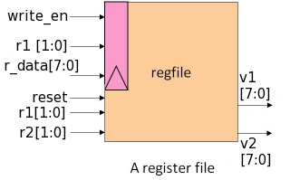
The above figure shows the basic structure of our register file. From this figure, it can be inferred that a write is edge-triggered,
while a read is level-triggered. The implication of this is that if write_en is asserted before or on a given clock edge, the data at
r_data will not be stored into the register specified by r1 until the next clock edge. However, if either
r1 or r2 is asserted between clock edges, we would expect the output to appear at v1
or v2 within the same clock cycle.
The following waveform demonstrates this concept:

Question 5: Implement reg_file.v noting the information above. Provide the source code.
Useful Resources
| Deliverable |
- Submit your report for the questions above to the TA via e-mail by the due date before the beginning of the class. Also bring a hard copy in class.
- Answer all of the questions (5) found in the lab description.
- The report should be in a single PDF file (including answers to questions, verilog source code, graphs, screen-shots, etc).
There are many tools out there capable of integrating text and graphics and producing PDF files (OpenOffice does a pretty good job).
- Name your PDF file cse141L-lab1-LastName1-FirstName1-LastName2-FirstName2-LastName3-FirstName3.pdf with your group members' last names
and first names substituted for LastName1-3 and FirstName1-3, respectively.
- The subject line of your email should read "[CSE141L] Lab 2 Submission - LastName1, FirstName1 - LastName2, FirstName2 - LastName3, FirstName3".
|
Due: October 14 |