CSE 141L Homepage | Lab Overview | Lab Description | Useful Resources
| Deadline: | Oct. 8 at 6PM |
| Changes: |
|
Jump to: Part 1 | Part 2 | Part 3 | Part 4 | Part 5 | Part 6
We encourage you to also work in the CSE labs in the basement of the CSE building. Xilinx 10.1 should be installed on the windows partitions of all the computers in the lab. Please let us know (via the WebBoard) if you find lab computers that don't have Xilinx installed or have an older version of the software.
At AwesomeCore, we just bought a couple new Virtex4 XC4VLX15 FPGAs. To get you started, your manager has given you a Verilog file (adder.v) that describes a basic 8-bit adder. Look at the file and make sure you understand it thoroughly. After doing so, create a new project in Xilinx ISE that contains this adder. When creating the project, remember to set the correct device (Virtex4 XC4VLX15) and simulator (ISE Simulator) to avoid problems later.
| Q1 | Draw a schematic for adder.v. In your schematic, you should clearly show the function of the design by using flip-flops, various gates, a comparator, an adder, and wires. Try to infer a schematic from the Verilog source, but it is fine to use a generated schematic from Xilinx ISE as long as it is detailed enough. |
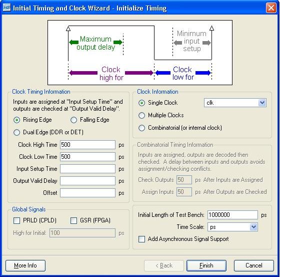
To see what is really going on, perform a behavioral simulation. You need to make a proper Testbench Waveform file as you did in the Xilinx tutorial. Use timing parameters in the figure below - it is equivalent to 1 GHz. Does it behave as you expected?
You might have noticed that output 'isOdd' is updated one cycle later than 'out'. (Stupid...who wrote this?) Anyway, it is a good opportunity to show your ability to tweak a design to get maximum performance. Modify the verilog file so that 'isOdd' is simultaneously updated with 'out'. Perform the same behavioral simulation you did in the previous step again. (Hint: You may want to examine blocking vs non-blocking assignment in Verilog.) Note: When updating your adder.v, both 'out' and 'isOdd' should be updated the cycle after the input(s) change, not two cycles later.
| Q2 | Include the modified version of adder.v. Also, draw a schematic for this modified adder. |
Now that you have verified that your adder is functionally correct, it is time to synthesize. In the synthesize stage, Xilinx ISE translates your Verilog design to what its backend stage (implementation stage) can understand. To synthesize a design, just double-click "Synthesize-XST" in the "processes" window. Xilinx ISE generates reports for each major stage. You can read them in the 'Design Summary' tab as shown in the figure below. Skim through the generated synthesis report.
| Q3 | How many flip flops are used for the design? How many LUTs does XC4VLX15 have, and how many LUTs does your design use? What is the 'estimated' achievable maximum frequency? (Ignore numbers in the figure below.) |

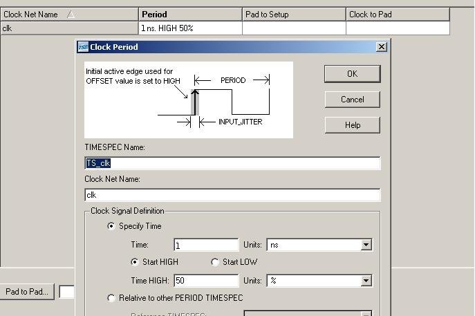
To actually program your FPGA, you need to "implement" your design. "Implement" is the term the Xilinx tools use for the stage which decides how to configure LUTs and networks of FPGA. For implementation, first you need to specify your timing constraints. You are targeting 1ns cycle time and 50% duty cycle as in the figure below. (You do not need to set 'clock-to-pad' and 'pad to setup' constraints.) With these constraints, Xilinx will generate a clock signal which alternates between high and low every 1ns. Then double-click "Implement Design". After implementation, Xilinx will generate a few reports. Skim through them.
If your timing constraint is unable to be met, you may get an an error during the "Place & Route" phase of implementation. Checking the 'static timing report' should give you a better idea of what your timing constraint needs to be changed to in order for the implementation to complete.
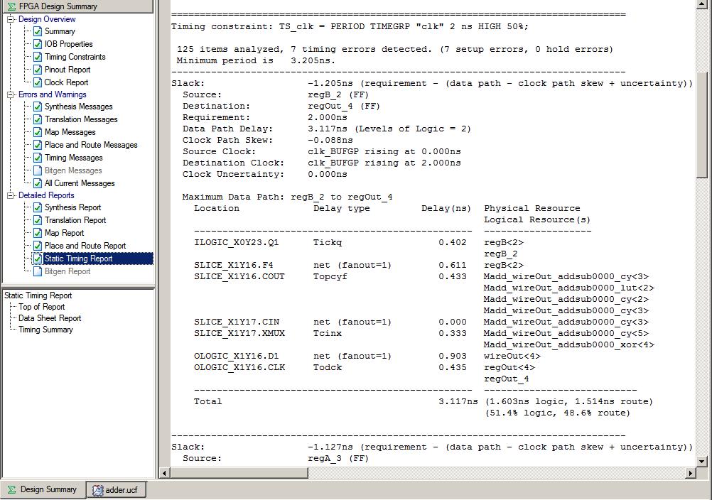
You can see detailed timing information in 'static timing report' (as in the picture below). In the report, you should look to see if you have any 'Slack' in your timing. Slack is the time delay difference between what you wanted (i.e. your timing constraints) and the actual delay. A positive slack implies that you met your constraints, while a negative slack implies just the opposite. To eliminate the negative slack, you need to loosen your timing constraints. If you have positive slack, you will not see all the detailed information shown in the screenshot below.
As you will learn in lecture, combination logic is implemented by using lookup tables (LUTs) in FPGAs. Input/Output Blocks (IOBs) provide an interface from the external world to the FPGA. Each FPGA has a set number of LUTs and IOBs that are available for use so you should be careful to not exceed that number when you are designing your processor.
| Q4 | How many 4-input LUTs and IOBs are used? |
| Q5 | Was your initial time constraint met? If not, what is the minimum achievable cycle time? Change you timing constraints and implement your design again, making sure there is no negative slack in your implementation. In the figure above, the design has negative slack, which means it failed to meet timing constraints. What is the maximum operating frequency of your adder? Compare the frequency with 'estimated' minimum frequency you got in Q3. What caused the difference between the two values? (Hint: See how much time is used for logic and delay respectively.) |
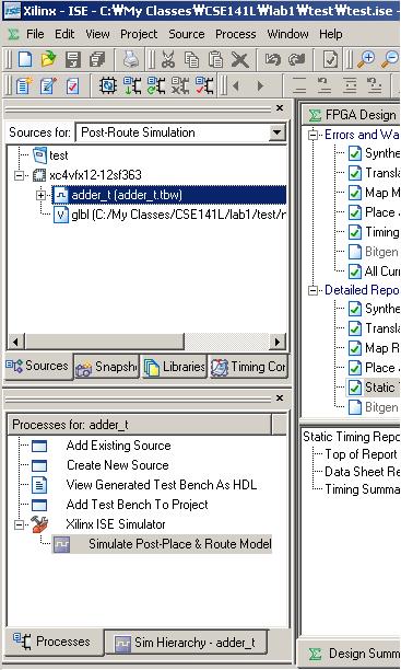
In order to prove that your adder works at a certain frequency, you need to do a post-route simulation. By comparing the results of your behavior simulation with post-route simulation, you can verify the validity of your implementation. Luckily, you can reuse the testbench from the behavior simulation you did earlier and the process for running the simualation is very similar. Select 'Post-route simulation' instead of 'Behavioral simulation' as shown in the following figure, then double-click 'Simulate Post-Place & Route Model'.
| Q6 | Include the two simulation results (behavioral and post-route) in your report. Are they the same as each other? If not, why are they different? If needed, modify the test bench file and make sure post-route simulation works correctly. (Hint: Behavioral simulations do not have a sense of frequency while post-route simulations do.) |
Generally, the bigger and more complex your design is, the slower it will be. It is important to understand the main causes of this phenomenon:
| Q7 | Since your FPGA has limited hardware resources and you are always concerned about your performance, you should try
to characterize the cost of different sizes of adders. Fill out the following table with information on adders ranging
from 8 bits to 64 bts.
|
After synthesizing your multiplier, skim through the generated synthesis report. You should notice that a new device, DSP48s, are being used in your multiplier. Since multipliers are frequently used in digital designs, most Xilinx FPGAs include a few highly optimized multipliers such as the DSP48.
| Q8 | Fill out the following table for 32-bit, 48-bit, and 64-bit multipliers. Note that some mulipliers might not fit in
the XC4VLX15 due to their demands on resources. In such cases, explain the reason.
|
||||||||||||||||||||
| Q9 | Draw two graphs for adders and multipliers with bit width on the X axis and frequency (MHz) on the Y axis. |
| Q10 | Design an experiment that answers some kind of question you have about the tool, and report on the results. |