Project Homework #2
Due: November 5, 1:00 PM
In this assignment, you are asked to implement a simulated annealing based
placement algorithm for a standard-cell based design. The layout of the
chip will include only two rows. The cells in each row will be selected
according to the partitioning algorithm implemented in your first assignment.
Those of you who could not complete the first assignment should use an already
partitioned version of the circuit provided. However, you are urged to use the
partitions created by your own algorithm.
Algorithm Details and Input Output Specification
Since you are going to be using the results attained through the program
developed in your first assignment, the input specification of your program is
exactly the same as the first assignment.
- Your program should initially partition the circuit into two subcircuits
and the cells in each partition should be printed out. For example:
- Partition 1: 1 5 7 8 9
- Partition 2: 0 2 3 4 6
- Create an initial placement by just using the initial ordering of the
components.
- Calculate and print out the initial cost (total wire length required by
this placement). In doing so, you should use the following distance
specifications.
The specification of the standard cells is shown in the
following figure,
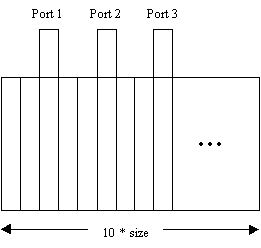 where size is the size of the component defined in the first
assignment, and the port numbers correspond to the port numbers given in the
circuit connectivity matrix.So, there will be one port for each 3 unit distance
on the cell and all cells provided will satisfy the following condition:
where size is the size of the component defined in the first
assignment, and the port numbers correspond to the port numbers given in the
circuit connectivity matrix.So, there will be one port for each 3 unit distance
on the cell and all cells provided will satisfy the following condition:
3* (number of ports) <= 10 * size
All components are left aligned and empty space is always at the right hand side of the components.
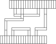
Here is an example of wire length estimation. The total
estimated wire length for the following figure is 32. While calculating the
wire length, you need to consider only the horizontal wires.
- Simulated annealing algorithm.
- Choose initial T as the length of one of the rows in your circuits. The
constant that is used to modify the temperature should be chosen as 0.9.
- Choose a component randomly. The component can be chosen from any of the
rows. You might first choose the row randomly and then choose a component
from that row. Then change the position of the selected component to a
random location in the same row. Changing the location may entail pushing
the intervening blocks appropriately. If a block is moved to the right,
intermediate blocks will be pushed left, and vice versa. The distance
calculations for the connections of all intervening blocks will be affected
consequently. Calculate the new estimated wire length. Naturally, if the
wire length is less that the initial wire length, you accept this move. If
the new wire length is larger than the initial wire length, you calculate
the quantity e-(new cost - old cost) / T. This quantity must be
between 0 and 1. At this point you pick a random number between 0 and 1, and
if the number that you picked is less than the above quantity, you keep this
move (keep a bad move, hoping to avoid a local minimum), otherwise ignore
the last move.
- You need to repeat step 2 for a number of times before changing the
temperature. Please consider the heuristics given in your text for
selection of the number of repetitions. That is for a circuit with N
components, the number of iterations inside Metropolis (i.e. the coefficient
M) shold be (N*N)/2. In this case the coefficient beta is equal to 1.
- Decrease the temperature by using the formula, Tn = 0.9 *
To. Then go to step 2. The algorithm should terminate when the
improvement between the successive iterations (calls of Metropolis, not
iterations inside Metropolis) is below 2% three times in a row.
- For each temperature, print out the current temperature and the final wire
length for that temperature.
- When the algorithm terminates, print out the final partitions
together with the final estimation of the wire length.
- While implementing the algorithm, do not forget the fact that you will be
using the output of this assignment as the input of your next assignment.
Here are the two different circuit connectivity matrices.
- Circuit
1
Partitions:
Partition0: 6 ->0 9 2 5
Partition1:
11 ->7 8 4 10 1 6 3
Expected final wirelength: 290
- Circuit
2
Partitions:
Partition0: 356 ->13 133 121 3 25 127 115
58 163 125 114 11 99 128 112 96 117 124 111 154 110 130 109 23 118 19 135 27
107 94 106 31 119 143 105 159 46 147 38 160 93 41 42 43 129 101 136 47 48 49
50 51 52 141 61 145 155 57 153 59 97 92 62 63 64 158 157 67 68 69 70 100 102
73 74 75 76 77 78 131 9 81 82 83 84 21 86 87 88 120 90 40 137 161 29 7 95 123
113
Partition1: 336 ->33 44 30 15 195 80 35 72 116 126 1 134 60 98 85
132 6 65 0 103 10 138 139 140 36 142 89 144 79 146 53 148 149 150 151 39 91
152 54 156 56 55 37 104 66 162 122 164 165 166 167 168 169 170 171 172 173 174
175 176 177 178 179 180 181 182 183 184 185 186 187 188 189 190 191 192 193
194 2 4 8 108 12 16 18 20 24 26 28 32 34 5 71 17 45 14 22
Expected final
wirelength: 179668